
Introduction
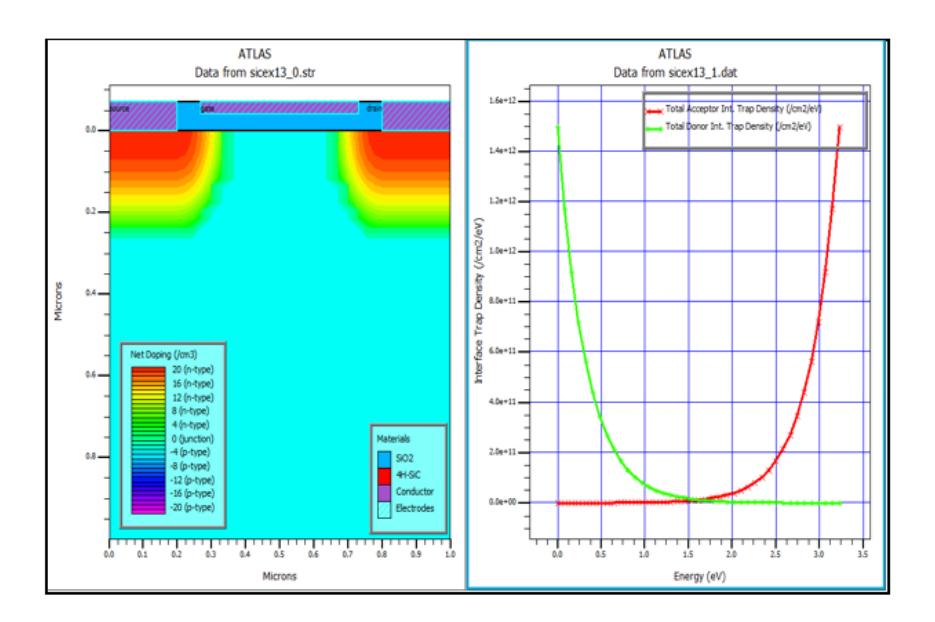
Silicon carbide (SiC) based metal-oxide-semiconductor field-effect transistors (MOSFETs) have superior characteristics, such as high thermal conductivity and a high breakdown electric field, which make them suitable for power device applications like power supplies, switches, automotive electronics, AC motors, and photovoltaic inverters [1-3]. SiC is primarily used in high-temperature and high-performance power semiconductor devices due to its wide bandgap and enhanced electric field [4, 5]. Presently, high-power technology requires a high-quality, reasonably thick gate oxide to support a gate voltage (VG) above 15 V [6]. It has been reported that a significant current flow, known as the Fowler-Nordheim tunnelling gate, occurs when MOSFETs are operated at high gate voltages. This current flow tends to damage the oxides [6-8] and the effect is significantly noticeable in thin oxide films [9]. As a result, a thermally grown thick silicon dioxide (SiO2) gate of good quality is critical for high-power device applications. Oxides grown on 4H-silicon carbide (SiC) have been seen to exhibit high near-interface and interface charge densities [10-13] due to the existence of carbon clusters, silicon oxycarbides and the incomplete elimination of Si-, C-dangling bonds. Currently, the largest issue preventing SiC device operation, especially at high voltage, is high interface trap densities. Manufacturers can improve their procedure and create better SiC devices by creating a density profile for the interface traps (Dit) and selecting the optimal gate oxide thickness along varied gate voltages [14, 15].
SiC MOSFETs continue to struggle to operate at their optimal performance due to the interaction between the SiC and the gate oxide. To understand the factors that restrict the inversion layer mobility in these devices, a substantial amount of study on SiC-based MOSFETs has been performed utilizing data from the Silvaco ATLAS Technology Computer-Aided Design (TCAD) based simulation software [16, 17]. The field effect mobility is significantly influenced by the energy distribution of interface traps at the MOS interface, which is caused by the large number of traps at the SiO2/4H-SiC interface. The major restrictions on the inversion layer mobility of SiC MOSFETs are considered to be caused by constraints like Coulomb and phonon scattering, which are associated with the high, intermediate, and low electric field areas [18-20]. In general, 'carrier mobility' is an important parameter which impacts the operation speed and high-frequency response character of solid-state electronic devices (e.g., switch transistors, logic gates, and demodulators) [21]. Hole mobility is the term used in semiconductors to describe analogous mobility for holes [22].
Generally, Matthiessen's rule, which serves as the foundation for understanding carrier transport characteristics in MOSFET inversion layers, has been used to categorize scattering elements. According to Matthiessen's rule, the cumulative scattering rate is calculated by adding the scattering rates of all the different scattering components [23]. Examples include ionized impurity scattering in surface phonon scattering, bulksemiconductor scattering, Coulomb scattering, and surface roughness scattering at the SiO2/4H-SiC interface. This work presents theoretical and simulation research on the effects of gate voltage and oxide thickness on the movement of electrons at the 4H-SiC/SiO2 interfaces. The discussion in this work will be confined to the movements of electrons in the inversion layer at the 4H-SiC/SiO2 interfaces and the factors influencing them.
Methodology
Based on voltage ratings, Table 1 shows the main uses for SiC-MOSFETs in power supplies and motor controllers. The SiC-based semiconductor industries require a high-quality thick SiO2 gate oxide, primarily for high-voltage applications above 600 V, to reduce device production costs and process steps [6, 24]. Eq. (1) presents the dielectric constant ratio for oxide as an insulator and 4H-SiC:
\[\varepsilon_{ratio} = \frac{\varepsilon_{r,SiC}}{\varepsilon_{r,ox}}\] (1)
where ,= 10 and , = 3.9 are the dielectric constants of silicon carbide (SiC) and its oxide, respectively. As stated in Eq. (3), the electric field in the gate oxide is expected to be roughly 2.5 times greater than in SiC during operation while the device is in the blocking state [6, 25]. The electric field in the association between SiC and gate oxide can be determined using following equation:
\[E_{SiC} = E_{ox}(\frac{\varepsilon_{r,ox}}{\varepsilon_{r,SiC}}) \tag{2}\] where ESiC represents the silicon carbide electrical field, while Eox refers to the gate oxide electric field. The highest possible SiC surface electrical field, ESiC, in the SiO2/4H-SiC structure must be maintained at or below 1.2 MV/cm for safe operational functioning. This is comparable to the gate oxide's 3 MV/cm maximum surface electric field [8].The following equation relates the electric field with gate voltage oxide to gate oxide thickness:
\[t_{ox} = \frac{(V_G - \phi_{ms})}{E_{ox}} \tag{3}\] where ms denotes the work-function distinction between the semiconductor and the metal, tox denotes the gate oxide thickness, and VG is the voltage applied to the gate.
Given that ms= 0.45 V and Eox = 3 MV/cm are the highest possible electrical field limitations for 4H-SiC-based gate oxide, a gate voltage of 15 V and a gate oxide thickness of 50 nm are needed to maintain gate voltage [26].
Within the lattice structure, electrons and holes are known to move freely. This is due to the fact that they have many scatterings with the atoms. The ability of an electron (or charged carrier) to move through a solid material while being influenced by an electric field is known as electron mobility [21].
\[\mu = \frac{(V_d)}{E} \tag{4}\]
Eq. (4) defines the mobility, where µ is the charge carrier mobility, vd is the drift velocity, and E is the electric field. Another important property that distinguishes conductors and semiconductors is electrical conductivity, σ [27, 28] as stated in Eq. (5):
\[\sigma = ne\mu_e \tag{5}\]
The elementary charge, charge carrier density, and temperature-dependent carrier mobility are denoted as e, n, and µe, respectively in Eq. (5). One of the primary parameters used to distinguish between conductors and semiconductors is the dependency of conductivity on temperature [27]. Then, resistance is given by Eq. (6) [29]:
\[R = \frac{l}{\sigma A} \tag{6}\] where l is the sample's length, A denotes the cross-sectional area, and σ is the conductivity. Using Eq. (5), the value of σ is substituted for the electron mobility in the formula to get an expression for resistance-electron mobility dependence (Eq. (6)).
Results and Discussions
Table 1 shows the major applications of SiC-MOSFETs in high voltage ratings. The majority of SiC-based power devices designed for high voltage applications typically have a gate voltage rating ranging from 15 V to 18 V in order to ensure the device's optimal safety. Table 2 shows the derived gate oxide thickness requirement using Eq. (3) for high-power applications in accordance with the gate voltage rating.
Table 1 Examples of major applications of SiC-MOSFETs in high voltage ratings [30].
| Applications | Voltage Rating |
|---|---|
| Home-based electronic appliances | 600 V |
| Charger application for electric vehicles | 600 V-1200 V |
| Electric vehicle (power train) | 500 V-1000 V |
| Renewable energy applications (inverters for photovoltaic and wind farms) | 1 kV-6.5 kV |
| AC based traction/drives | 2.5 kV-6.6 kV |
Table 2 Gate voltage and calculated gate oxide thickness requirement for high power applications.
| Gate Voltage (V) | Calculated Gate Oxide Thickness (nm) |
|---|---|
| 15 | 48.5 |
| 16 | 51.8 |
| 17 | 55.1 |
| 18 | 58.5 |
Conversely, the electric field in the oxide increases as the gate voltage increases, eventually leading to oxide breakdown [8, 31]. This observation is noteworthy, as it demonstrates a positive correlation between the thickness of the oxide layer and the threshold voltage of MOSFETs [9]. Therefore, the presence of a stable gate oxide with a thickness over 50 nm is crucial for high-power devices.
Figure 1 shows the electron mobility against electric field, which is contributed by Coloumb scattering and surface phonons. With a significant quantity of interface traps located in the 4H-SiC/SiO2 region, an enhancement-mode n-channel 4H-SiC MOSFET is used to illustrate how mobility components affect overall inversion layer mobility. The acceptor and donor interface state density distributions are presented with the simulated 2D net doping profile of 4H-SiC MOSFET (Figure 2).
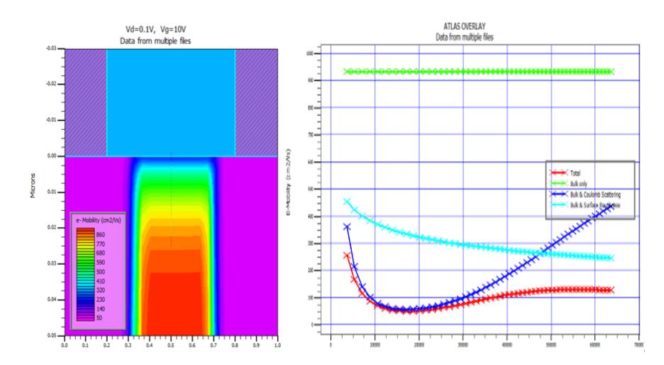
Graph of electron mobility versus electric field obtained from Silvaco ATLAS TCAD.
Electric field distribution in the designed 4H-SiC MOSFET and plot of electron mobility against the electric field obtained from Silvaco ATLAS TCAD.
Based on Figure 3, the results show that the total inversion layer mobility is greatly influenced by surface phonons at the interface charges as well as Coulomb scattering. However, the electron mobility due to Coulomb scattering and surface phonons improves as the oxide thickness and gate voltage increase. At thicknesses below 45 nm and voltage levels of 15 V and 16 V, electron mobility due to Coulomb scattering tends to be lower but increases as the thickness and gate voltage increase. It is well known that silicon carbides, and 4H-SiC in particular, have lower channel mobility than Si in a MOSFET structure. The primary source of this phenomenon is the accumulation of electric charge at the interface between SiO2/4H and SiC, resulting from Coulomb scattering and the presence of a high density of traps at the interface. Silvaco ATLAS TCAD provides an alternative inversion layer mobility model designed specifically for 4H-SiC that incorporates trapped charge Coulomb scattering at the SiO2/4H-SiC interface, ionized impurity scattering, and surface phonon scattering in bulk semiconductors [18-20].
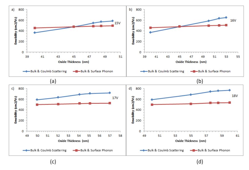
Limiting factors in SiC MOSFETs at varied gate voltage: (a) 15 V, (b) 16 V, (c) 17 V, (d) 18 V.
Figure 4 shows the total electron mobility due to the above-mentioned limiting factors; the data was obtained from observation at each gate voltage (VG), i.e., 15 V, 16 V, 17 V, and 18 V, respectively. From the graph, it appears that e-mobility increases as oxide thickness and gate voltage increase. However, the rise of e-mobility is noticed to be saturated at a certain estimated oxide thickness, which is considered the ideal oxide thickness for the respective gate voltages.
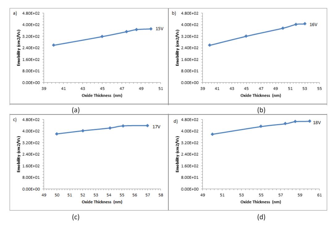
E-mobility against oxide thickness graph at varied gate voltage: (a) 15 V, (b) 16 V, (c) 17 V, (d) 18 V.
Table 3 shows the percentage difference between the calculated values and the extracted values from the saturation point. The percentage difference is below 1%, which is an assertion from theoretical and experimental research about the role of optimized oxide thickness and gate voltage on the movement of electrons at the 4H-
SiC/SiO2 interfaces. Also, for semiconductors to work well in a high-performance electronic application, the gate oxide needs to be relatively thick. A thicker oxide is able to withstand a higher supply voltage.
Thick gate oxide transistors are utilized to ensure minimal leakage current and to provide a higher voltage swing, while thin oxide transistors are employed whenever feasible to attain limited area and low power consumption. The VG of a MOSFET depends inversely on the capacitance in the oxide layer (between the gate and substrate), Cox, however, Cox itself reduces with the increase of Tox based on the gate-insulator capacitance/unit area equation, Cox = εox/Tox [32]. Hence, the gate voltage of a SiC MOSFET is directly proportional to the thickness of the oxide layer.
| Gate Voltage (V) | Calculated | Extracted | Percentage |
|---|---|---|---|
| Gate Oxide Thickness (nm) | Gate Oxide Thickness (nm) | Difference (%) | |
| 15 | 48.5 | 48.6 | 0.21 |
| 16 | 51.8 | 51.8 | 0.00 |
| 17 | 55.1 | 55.2 | 0.18 |
| 18 | 58.5 | 58.6 | 0.17 |
Table 3 Calculated and extracted gate oxide thickness at the saturation point with percentage difference.
Figure 5 depicts the gate oxide thickness in relation to optimized gate voltages, with the electron mobility increasing as the voltage, Tox, and VG increase. Based on Figure 5, it appears that a voltage of 18 V with a 58.5 nm oxide thickness has the highest E-mobility (466 cm2 /Vs) as compared to other voltages.
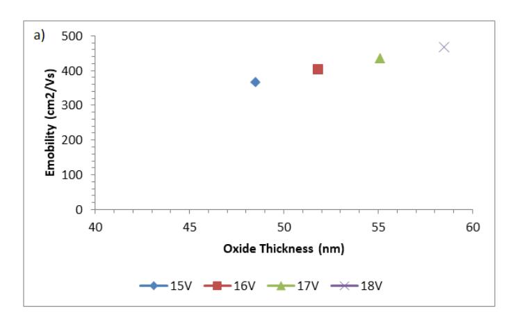
Graph of electron mobility against oxide thickness at estimated values of oxide thickness.
Figure 6 shows the correlation between the electric field and oxide thickness based on varied gate voltages. The graph shows that the electric field decreases as tox increases. Moreover, Eq. (6) also demonstrates that the electric field exhibits an inverse relationship with the thickness of the oxide. Thus, it may be deduced that substantial electric fields can form in the oxide even at low voltages if the oxide layer is thin. On the other hand, based on the graph, it is observed that the oxide's electric field increases as the gate voltage rises. Also, it was noticed that at 50 nm of oxide thickness, the electric field of 18 V (>6E5 V/cm) is higher as compared to 15 V, 16 V, and 17 V, which have electric fields below 6E5 V/cm.
The graphs for oxide thickness against resistance in relation to various gate voltages are shown in Figure 7. The value of resistance is calculated based on Eqs. (4), (5), and (6). The resistance in the inversion layer decreases as the oxide thickness increases; hence, it can be concluded that enhancing oxide thickness tends to decrease Coulumb scattering and surface phonon effects, which eventually increase electron mobility. From the graph, it is also noticeable that the resistance becomes constant at a certain Tox point, which acts as the ideal Tox for the respective gate voltages. Based on Figure 8, the graph represents the decline in the trend of resistance with the optimized oxide thickness in relation to the gate voltages. For a voltage of 18 V with a 58.5 nm oxide thickness, it has a lower resistance compared to other voltages, and this shows that an 18 V gate voltage is preferable for high voltage applications without compromising the oxide quality.
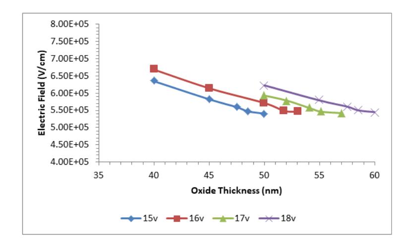
Electric field against oxide thickness graph.
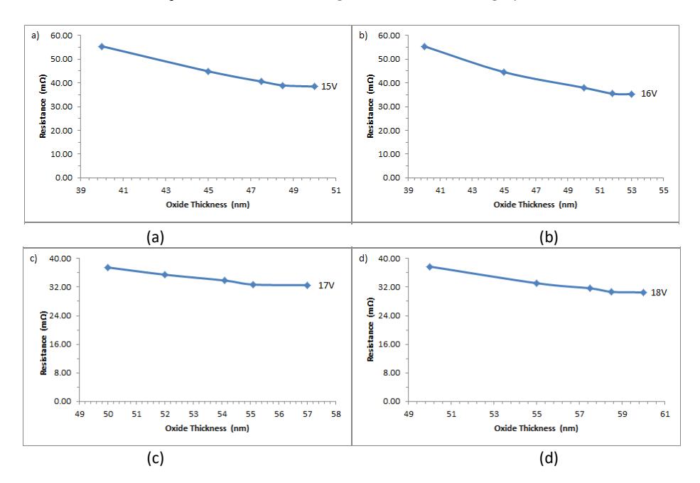
Resistance against oxide thickness at varied gate voltages: (a) 15V, (b) 16V, (c) 17V, (d) 18V.
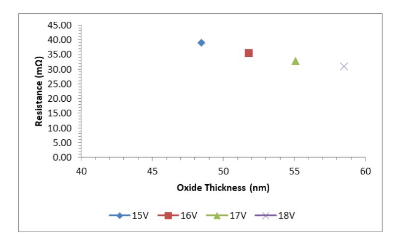
Resistance against estimated oxide thickness.
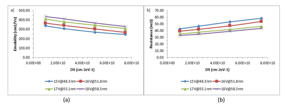
Interface trap density at varied gate voltage@oxide thicknesses: (a) E-mobility, (b) resistance.
Figure 9(a) depicts the increase in e-mobility versus interface trap density (Dit) with the optimized VG and Tox values. This result affirms that the high density of interface traps is a major contributor to the SiC MOSFETs' poor inversion channel mobility. Hence, an enhanced gate voltage is essential to overcome the large density of interface traps. Figure 9(a) shows that 18 V at Tox = 58.5 nm provides the highest electron mobility. The correlation between resistance and interface trap density (Dit) is depicted in Figure 9(b), with resistance increasing as Dit increases. Thus, the reduction of Dit during gate oxide growth is necessary to obtain the optimum quality of SiC MOSFETs [33].
Conclusion
In summary, the effects of electron mobility and resistance on varied oxide thickness (Tox) in the 4H-SiC/SiO2 inversion layer with enhanced gate voltages were observed in this work. The results of this work revealed that at low resistance, the E-mobility increases with gate voltage and oxide thickness, which saturates at the point of value. It can be seen that there is a strong correlation between the electron mobility and Dit because the MOSFETs' electron mobility significantly decreased as the Dit values increased. Hence, an enhanced gate voltage is required to overcome the high density of interface traps, which shows that 18 V at Tox = 58.5 nm provides the highest electron mobility. In this work, Coulomb scattering and surface phonons at the SiC MOSFET inversion layer are widely considered to be limiting factors of electron mobility in the inversion region. The outcomes of this study showed that simulation-based oxide thickness and calculated values of oxide thickness have the least variation below 1%, supporting claims made in both theoretical and simulation investigations about the effects of oxide thickness and gate voltages on the movement of electrons at the 4H-SiC/SiO2 interfaces. The results in this work indicate that understanding the electron mobility effect on oxide thickness in the SiC MOSFET inversion layer according to gate voltage is important, particularly in achieving an ideal 4H-SiC/SiO2 interface for highpower applications. The development of the power electronics industry is strongly linked to its capacity to adjust to emerging materials and technologies, to satisfy the continuously increasing need for effective electronic systems. SiC-based power semiconductor devices are expected to play a crucial role in driving progress in the field of power electronics during this development. Wide-bandgap semiconductors have the capacity to transform several sectors, particularly high-voltage applications, by offering smaller and more efficient systems.
Acknowledgements
The funding for this work was provided by the Fundamental Research Grant Scheme (FRGS) under grant number FRGS/1/2020/STG05/UniMAP/02/7(9003-00862) from the Ministry of Higher Education Malaysia. Sincere gratitude is extended to Universiti Malaysia Perlis for its assistance with this work and Universiti Teknologi MARA(UiTM) (Pulau Pinang) for providing access to the software applications.
Compliance with ethics guidelines
The authors declare that they have no conflict of interest or financial conflicts to disclose.
This article does not contain any studies with human or animal subjects performed by any of the authors.