
Introduction
Graphene, a two-dimensional carbon allotrope, has garnered significant attention in recent years due to its exceptional properties, including high electrical conductivity, mechanical strength, and thermal stability (Xu et al., 2013; Khan et al., 2021). These unique characteristics make graphene a promising material for various applications, ranging from electronics and energy storage to biomedical devices and composite materials. The synthesis of high-quality graphene films is crucial for unlocking its full potential in these diverse fields. Among the various synthesis techniques, plasma sputtering has emerged as a promising method due to its scalability, versatility, and compatibility with different substrates (Fu et al., 2018). However, achieving precise control over the synthesis parameters is essential to obtain graphene films with desired properties. This study aims to investigate the optimal parameters for synthesizing graphene using the plasma sputtering technique and validate the identity of the synthesized coatings using Raman spectroscopy analysis.
Previous studies have explored the influence of different process parameters (Table 1), such as gas composition, plasma power, and deposition time, on the properties of synthesized graphene films (Li et al., 2016). However, there remains a need for systematic optimization of these parameters to achieve reproducible and high-quality graphene coatings. Raman spectroscopy has emerged as a powerful tool for characterizing graphene and other carbon-based materials (Roy et al., 2021). By analyzing the vibrational modes of carbon atoms in the graphene lattice, Raman spectroscopy can
provide valuable information about the structural quality, layer thickness, and defect density of graphene films. Several studies have utilized Raman spectroscopy to characterize graphene synthesized using various methods, including CVD, chemical reduction, and plasma sputtering (Abdelrahman et al., 2023). The distinctive Raman spectra of graphene, characterized by the presence of D, G, and 2D peaks, enables precise identification and quantification of graphene layers and defects.
| Author and Year | Focus of Study | Key Findings | ||
|---|---|---|---|---|
| Li et al., 2016 Graphene properties | Discovered the exceptional properties of graphene, such as high electrical conductivity, mechanical strength, and thermal stability, opening avenues for diverse applications. | |||
| Abdelrahman et al., 2015 | Plasma sputtering technique | Explored the potential of plasma sputtering as a promising technique for synthesizing graphene due to its scalability, versatility, and compatibility with various substrates. | ||
| Wimalananda et al., 2017 | Parameter optimization in plasma sputtering | Investigated the influence of parameters like gas composition, plasma power, and deposition time on the properties of graphene films synthesized using plasma sputtering. | ||
| Li et al., 2023 | Raman spectroscopy in graphene characterization | Discussed the utility of Raman spectroscopy in characterizing graphene and other carbon-based materials, providing insights into their structural properties, layer thickness, and defect density. | ||
| Yang et al., 2019 | Utilized Raman spectroscopy to characterize graphene synthesized with Raman spectroscopy in different methods, including chemical vapor deposition (CVD), chemical graphene synthesis reduction, and plasma sputtering, enabling precise identification and quantification of graphene layers and defects. | |||
| Yeh et al., 2019 | Systematic optimization in graphene synthesis | Emphasized the necessity of systematic optimization of parameters to achieve reproducible and high-quality graphene coatings using plasma sputtering, highlighting the importance of understanding the correlation between process parameters and graphene film properties. | ||
Table 1 Literature overview: graphene synthesis and characterization.
This study aims to fill gaps in the existing literature by systematically investigating the optimal parameters for synthesizing graphene using the plasma sputtering technique. This technique involves physically bombarding target atoms to synthesize and/or deposit them onto the sample surface. In this study, we employed a plasma-enhanced chemical vapor deposition (PECVD) reactor to synthesize graphene films using a mixture of acetylene (C₂H₂) and hydrogen (H₂) gases in a low-pressure plasma discharge environment. By conducting a comprehensive analysis of key factors, such as electric power, gas composition, and deposition time, we seek to identify the optimal conditions for producing high-quality graphene films. Additionally, the validation of graphene identity using Raman spectroscopy analysis will contribute to the understanding of structural properties and aid in distinguishing graphene from other carbon-based materials. The research findings are expected to provide valuable insights into optimizing plasma sputtering parameters for graphene synthesis, offering a pathway toward the reproducible and scalable production of graphene coatings. Furthermore, the characterization of graphene films using Raman spectroscopy will enhance our understanding of their structural integrity, defect density, and layer thickness, thus facilitating their potential applications in electronics, energy storage, and nanocomposites. Ultimately, this study aims to contribute to the advancement of graphene synthesis methodologies and pave the way for the development of novel graphene-based technologies with enhanced performance and functionality.
Theoretical Background
Mass Transport Equation (Kleijn et al., 2007): In chemical vapor deposition (CVD), the transport of gas species to the substrate surface is described by Fick's laws of diffusion. Fick's second law, which is commonly used to model mass transport in CVD processes, is expressed as follows (Eq. (1)):
\[\frac{dc}{dt} = D \frac{d^2C}{dz^2} \tag{1}\]
In the mass transport equation used to describe CVD processes, represents the rate of change of the concentration (C) of a gas species over time, indicating how quickly the concentration changes in a given region. The parameter D is the diffusion coefficient, which quantifies how easily the gas species diffuses through the medium. Finally, 2 2 is the second derivative of the concentration with respect to distance (z), which reflects the spatial variation of the concentration gradient. Together, these terms model the dynamic behavior of gas species as they diffuse and interact within the CVD process environment.
Langmuir–Hinshelwood Mechanism (Moene et al., 1994): Surface reactions in CVD processes are often described using the Langmuir–Hinshelwood mechanism, which considers adsorption and reaction of precursor gases on the substrate surface. The rate of reaction (R) is proportional to the concentration of gas species in the gas phase (\(C_{gas}\)) and the fraction of the surface not covered by adsorbed species \((1-\theta)\). The Langmuir–Hinshelwood mechanism is represented as follows (Eq. (2)):
\[R = k_{ads}C_{aas}(1 - \theta) \tag{2}\]
In the Langmuir–Hinshelwood mechanism, the reaction rate (R) is influenced by several factors. The parameter \(k_{ads}\) represents the adsorption rate constant, which determines the efficiency of precursor gas molecules adsorbing onto the substrate surface. The term \(C_{gas}\) refers to the concentration of the gas species in the gas phase, which provides the source of reactants for the surface reaction. Lastly, \(\theta\) represents the fraction of the substrate surface covered by adsorbed species, while \((1-\theta)\) denotes the fraction of the surface available for further adsorption and reaction. These components collectively describe how surface reactions proceed in CVD processes.
Growth Rate Equation (Kleijn et al., 2007): The growth rate of the deposited film in CVD processes is influenced by factors such as precursor gas flow rates, temperature, and pressure. The growth rate equation relates the growth rate (v) to these process parameters and is commonly expressed as follows (Eq. (3)):
\[v = k \cdot P_{gas}^m \cdot T^n \tag{3}\] where v is the growth rate of the film, k is the growth rate constant, \(P_{gas}\) is the partial pressure of the precursor gas, T is the temperature, and m and n are empirical constants.
Principles of Hydrogenated Graphene Synthesis
Hydrogenated graphene, often referred to as graphane, involves the addition of hydrogen atoms to the carbon atoms in graphene, resulting in significant changes in its electronic and structural properties. This process can be achieved using various methods, including chemical vapor deposition (CVD), plasma-enhanced chemical vapor deposition (PECVD), and chemical reduction.
Plasma-Enhanced Chemical Vapor Deposition (PECVD)
In the PECVD process, hydrogenated graphene synthesis is facilitated by the generation of a plasma field, which enhances chemical reactions between the precursor gases (typically acetylene (\(C_2H_2\)) and hydrogen (\(H_2\))) and the substrate surface. The process generally involves the following steps:
- 1. Substrate Preparation: The substrate, often a glass slide or silicon wafer, is meticulously cleaned to remove any contaminants that might hinder the deposition process. This includes steps such as immersion in acetone and alcohol, followed by argon plasma treatment.
- 2. Plasma Generation: A low-pressure plasma discharge system is used to generate a plasma field by applying a high-frequency electric field to the precursor gases. This ionizes the gases, creating reactive species, including hydrogen radicals (H•) and acetylene ions (C<sub>2</sub>H<sub>2</sub>+).
- 3. Hydrogenation Reaction: The reactive species interact with the graphene surface, enabling the hydrogen atoms to bond with the carbon atoms in the graphene lattice. The reaction conditions, including electric power (50 W) and base pressure (2 x 10<sup>-2</sup> Torr), are crucial for controlling the degree of hydrogenation and ensuring uniform deposition.
- 4. Film Formation: The hydrogenated graphene film is formed on the substrate surface, with the hydrogen atoms saturating the carbon bonds. This process modifies the electronic properties of graphene, potentially making it an insulator or a semiconductor, depending on the degree of hydrogenation.
Chemical Reduction
Another common method involves the chemical reduction of graphene oxide (GO) in the presence of hydrogen-containing reducing agents, such as hydrazine (N2H4) or sodium borohydride (NaBH<sub>4</sub>). This method includes the following steps:
- 1. Synthesis of Graphene Oxide: Graphene oxide is synthesized through the oxidation of graphite, introducing oxygen-containing functional groups.
- 2. Reduction Process: GO is then dispersed in a solution with the reducing agent. Upon reduction, hydrogen atoms are introduced to the graphene lattice, reducing the oxygen groups and hydrogenating the carbon atoms.
- 3. Post-Processing: The reduced graphene oxide (rGO), now partially hydrogenated, is filtered, washed, and dried. The extent of hydrogenation can be controlled by varying the concentration of the reducing agent and reaction time.
Key Considerations
Hydrogen Concentration: The concentration of hydrogen in the plasma or reduction environment is critical. Too little hydrogen may result in incomplete hydrogenation, while too much can lead to over-saturation and potential damage to the graphene structure.
Temperature Control: Temperature plays a significant role in facilitating the hydrogenation reaction. Optimal temperatures ensure efficient bonding of hydrogen atoms to the graphene without causing unwanted structural defects.
Reaction Time: The duration of the hydrogenation process must be carefully controlled to achieve the desired degree of hydrogenation. Prolonged exposure to hydrogen radicals can lead to excessive hydrogenation and degradation of graphene's beneficial properties.
Method
Full two-level factorial with center points
In this study, we investigate the effects of electric power, the acetylene (C2H2)-to-hydrogen (H2) ratio, and discharge time on graphene synthesis using a low-pressure plasma discharge system. Using a full two-level factorial design with center points, we explore the entire feasible range of operating conditions to capture potential non-linear relationships (Table 2). Building on insights from previous research and acknowledging current technological limitations, our goal is to optimize the synthesis process, enhance graphene quality, and contribute to advancements in materials science and engineering.
Table 2 The details of factors, boundary levels, and symbols.
| Boundary Levels | |||||
|---|---|---|---|---|---|
| Factor | Low (-1) | Mid (0) (high) (+1) | Unit | ||
| Electric Power (A) | 60 | 80 | 100 | Watt | |
| Ratio of C2H2:H2 (B) | 30:70 | 40:60 | 50:50 | - | |
| Discharge Time (C) | 10 | 20 | 30 | Min | |
Overview of graphene synthesis
The principle of graphene film synthesis involves the use of a low-pressure plasma discharge system. This setup includes a plasma discharge chamber, gas inlets for acetylene and hydrogen, and a substrate holder. The process begins with thorough cleaning of the substrate, followed by its placement in the chamber where plasma sputtering occurs, resulting in the deposition of graphene films.
Graphene film synthesis was conducted using a PECVD reactor. The PECVD reactor used in our experiments operates by generating a plasma through radio frequency (RF) power. This process facilitates the dissociation of gas molecules and the subsequent deposition of carbon atoms onto the substrate. The reactor parameters were carefully controlled to optimize the graphene synthesis process. Specifically, acetylene (C₂H₂) and hydrogen (H₂) gases were introduced into the reactor with flow rates of 50 SCCM, and the RF power was set to 60-80 W with 13.56 MHz. The pressure within the reactor was maintained at 2 x 10⁻² Torr. This setup allowed for the efficient deposition of graphene films on the substrate surface.
During graphene synthesis, meticulous attention is given to the preparation and cleaning of the workpiece to ensure optimal conditions for growth. Initially, the glass slide undergoes a thorough cleansing regimen, starting with a 3 min immersion in acetone followed by a 10 min soak in alcohol. This dual-step cleaning procedure serves to remove any contaminants or impurities that may interfere with the subsequent deposition process. Subsequently, the workpiece is subjected to an additional purification step utilizing argon plasma treatment for 5 min, operating at an electric power of 50 W, and adjusting the base pressure to 2 x 10⁻² Torr. This additional cleaning step improves surface cleanliness and promotes better adhesion for subsequent graphene deposition. Following the preparatory stages, the controlled release of hydrogen gas and acetylene into a vacuum container is meticulously orchestrated, with parameters tailored according to various experimental conditions designed using sophisticated software tools such as the MiniTab program. The experimental design encompasses three factors, each with two levels, and is replicated twice with the inclusion of five center point tests, yielding a total of 21 experiments. Upon completion of the experimental phase, the treated workpieces are carefully stored in a humidity-controlled cabinet to maintain their pristine condition until further analysis in subsequent steps.
Contact Angle Measurement
In the assessment of surface properties during the graphene synthesis process, contact angle measurements play a pivotal role in evaluating surface wettability. Using a contact angle goniometer, the contact angle (θ) between a water droplet and the surface of the workpiece is meticulously assessed. Employing the sessile drop method, a precisely controlled volume of distilled water is dispensed onto the surface for testing using a small syringe. Subsequently, the workpiece is carefully maneuvered into position, ensuring parallel alignment with the base (stage) to optimize imaging clarity. A 40-microliter droplet of distilled water is then deposited perpendicularly onto the surface, with the base (stage) carefully raised to ensure contact without inducing foam formation. After adjusting the image sharpness to clearly delineate the water droplet's surface edge, the contact angle between the water droplet and the workpiece surface is measured using a specialized program integrated with the contact angle goniometer. Images are simultaneously captured for documentation and analysis on a computer screen. This meticulous procedure allows for a comprehensive evaluation of surface conditions and wettability, providing crucial insights into the effectiveness of plasma treatment and its impact on surface properties during graphene synthesis.
Surface Analysis using Atomic Force Microscopy in Graphene Synthesis
In the analysis of surface morphology during graphene synthesis, the use of an atomic force microscope (AFM) is paramount for obtaining high-resolution images and detailed topographical information. Prior to conducting AFM analysis, meticulous attention is given to ensuring the cleanliness and integrity of the specimen surface to prevent inaccuracies in measurements. The specimen must be free from any smudges or scratches, as these imperfections can potentially damage the delicate measuring needle and compromise the analysis of the workpiece surface. Additionally, it is imperative that the dimensions of the workpiece adhere to specified criteria, with a recommended size not exceeding 1 x 1 cm and a thickness not surpassing 3 mm to facilitate optimal imaging and analysis conditions. Images captured from surface scans are subsequently processed and analyzed using specialized software such as the Nanoscope SPM thickness analysis program. This comprehensive analysis allows for the thorough examination of surface morphology and topographical features, providing valuable insights into the structural characteristics of the synthesized graphene coatings. The AFM utilized for these analyses is the Nanoscope IIIa model, manufactured by Di Digital Instruments Company, renowned for its precision and reliability in nanoscale imaging and measurement.
Characterization of Graphene Film Structure and Purity using Raman Spectroscopy Analysis
In the comprehensive analysis of graphene film structure and purity, Raman spectroscopy plays a pivotal role by characterizing the crystal orderliness and identifying bonding configurations. Through the measurement of peak intensities corresponding to the disorder-induced vibration mode (D-Band) and the in-plane stretching mode (G-Band), insights into the degree of structural disorder and the purity of synthesized films are obtained. This analysis is facilitated by focusing an argon laser onto the desired surface and utilizing a microscope for precise adjustment and positioning. The Lab Spec program operates the Raman spectroscopy system, facilitating data acquisition and analysis. The resulting Raman peak graph provides a graphical representation of intensity versus Raman shift, offering valuable information regarding the composition and structural integrity of the analyzed material. The instrument utilized for these analyses is the T64000 model Raman spectroscopy system, manufactured by Horiba Jobin Yvon Company, France, renowned for its precision and reliability in mechanical properties analysis.
The synthesized graphene films were analyzed using Raman spectroscopy to assess their structural properties. The Raman spectra exhibited two key peaks: the disorder-induced vibration mode (D-band) and the in-plane stretching mode (G-band). The D-band, which is typically associated with defects or disorder in the carbon structure, was observed around 1,300–1,350 cm⁻¹. The G-band, representing the sp² hybridized carbon atoms in graphene, appeared near 1,580– 1,600 cm⁻¹. These peak positions can vary slightly depending on the specific synthesis conditions and structural characteristics of the material. In addition to Raman analysis, surface morphology was assessed using a Nanoscope SPM, offering high-resolution imaging for further characterization.
Results
Surface Wettability Analysis and Contact Angle Measurements Following Plasma Treatment
The assessment of the contact angle between water droplets and the surface of the workpiece provides valuable insights into the surface properties and wettability alterations induced by plasma treatment. Visual inspection of the glass slides post-plasma application reveals a distinct cloudy yellow hue attributed to the presence of acetylene gas, and the intensity of coloration increases with prolonged discharge time. The contact angle measurements, conducted using the sessile drop method, indicate notable changes in surface characteristics. Although summarizing trends across all conditions may prove challenging, comparing contact angle values before and after plasma application is useful to elucidate significant alterations in surface wettability. The detailed results are presented in Table 3, providing a comprehensive understanding of the plasma treatment's impact on the workpiece's surface properties.
| Sample | Left Contact Angle (°) | Right Contact Angle (°) | Average Contact Angle (°) |
|---|---|---|---|
| 1 | 51.38 | 59.06 | 55.22 |
| 2 | 60.56 | 58.69 | 59.62 |
| 3 | 55.36 | 59.75 | 57.55 |
| 4 | 63.67 | 66.28 | 64.97 |
| 5 | 69.1 | 64.79 | 66.95 |
| 6 | 58.76 | 66.48 | 62.62 |
| 7 | 63.24 | 65.18 | 64.21 |
| 8 | 57.79 | 54.58 | 56.19 |
| 9 | 69.01 | 72.82 | 70.92 |
| 10 | 63.58 | 60.39 | 61.98 |
| 11 | 62.16 | 65 | 63.58 |
| 12 | 66.54 | 65.35 | 65.95 |
| 13 | 60.32 | 67.48 | 63.9 |
| 14 | 61.33 | 59.86 | 60.6 |
| 15 | 64.64 | 64.76 | 64.7 |
| 16 | 69.33 | 69.59 | 69.46 |
| 17 | 45.3 | 54.49 | 49.89 |
| 18 | 68.42 | 66.17 | 67.29 |
| 19 | 68.43 | 66.17 | 67.3 |
| 20 | 67.72 | 65.14 | 66.43 |
| 21 | 46.17 | 39.28 | 42.73 |
Table 3 Contact angle measurements before and after plasma treatment.
The provided table presents contact angle measurements (in degrees) for 21 samples, with values recorded for both the left and right sides of each sample, as well as the calculated average contact angle. The variability in contact angles across samples suggests diverse surface properties, potentially influenced by factors such as surface treatment, roughness, and material composition. Although some samples exhibit consistent contact angle measurements, outliers indicate potential surface irregularities or anomalies requiring further investigation. This comprehensive dataset underscores the importance of contact angle analysis in evaluating surface wettability and highlights the need for meticulous characterization in graphene synthesis and related research endeavors.
Analysis of Workpiece Morphology and Thickness Variation Following Plasma Treatment
To assess the morphology of the workpiece post-plasma treatment, a systematic procedure was followed to ensure accurate measurement and characterization of the synthesized graphene film. Specifically, 1 cm-2 sections of the workpiece were selected for analysis, marked with distinct symbols to denote experimental conditions, and subsequently examined using an atomic force microscope (AFM), as depicted in Figure 1. The AFM analysis involved measuring the film thickness along the plane at five predetermined locations, with the horizontal distance values (referred to as "Vert Distance") displayed on the processing screen and serving as film thickness indicators. The average thickness of the synthesized film was then determined by calculating the mean of these measurements. Notably, the analysis revealed a discernible trend wherein the average thickness of the workpiece increased with prolonged discharge time, suggesting a direct correlation between processing parameters and film thickness, as summarized in Table 4. These findings underscore the important role of these meticulous characterization techniques in elucidating the impact of plasma treatment conditions on the structural properties of synthesized graphene films.
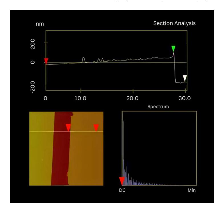
Graphene film thickness analysis using atomic force microscopy.
Statistical Analysis of Experimental Factors Influencing Average Film Thickness in Graphene Synthesis
Table 4 shows the average film thickness obtained by running the experiment under various testing conditions. The analysis of variance (ANOVA) displayed in Table 5 shows the relative significance of each main factor. To assess the dataset's fit, R-squared and adjusted R-squared statistics were also examined. Additionally, each main effect and its interaction were considered statistically significant if the p-value was less than 0.05. The analysis shows discharge time (C) and the ratio of C2H2:H2 (B). The average film thickness was influenced by the interplay of variables C and B. The R2 result demonstrates that the model explains 92.76% of the variance in the melt front time, demonstrating that the model effectively fits the data. The residual plot of the average film thickness and the normal probability plot of the residuals are shown in Figure 2. In the residual plots, the residuals of the response were randomly dispersed around zero. The observation points (blue dots) in the normal probability plot were randomly dispersed, indicating that the process parameters in this investigation followed a normal distribution and were independent when comparing the residuals to the fitted values. The histogram of the residuals is approximately symmetric. Regarding the residuals versus the order, no clear pattern is observed in the residuals.
The D/G ratio obtained from Raman spectroscopy is a pivotal indicator of the structural quality of graphene films, reflecting the degree of disorder within the material. Table 4 demonstrates that the D/G ratio across different experimental conditions ranges from 0.72 to 0.88. This variability highlights the influence of synthesis parameters on the film's structural integrity. Generally, a lower D/G ratio suggests higher graphene quality with fewer structural defects, whereas a higher ratio indicates increased disorder. The results show that lower electric power (60 W) and a higher C₂H₂ to H₂ ratio (30:70) typically correlate with lower D/G ratios, reflecting improved graphene quality.
Conversely, higher electric power (100 W) and a 50:50 gas ratio yields slightly higher D/G ratios, potentially indicating a higher level of defects or incomplete graphene formation.
Additionally, the impact of discharge time on the D/G ratio is evident from the data. Extended discharge times (30 min) tend to produce graphene films with higher D/G ratios, suggesting increased disorder or roughness. This contrasts with shorter discharge times (10 min), which generally result in lower D/G ratios and better film quality. The findings underscore the importance of optimizing process parameters, including the electric power, gas ratio, and discharge time, to achieve desired graphene film characteristics. By adjusting these parameters, researchers can effectively tailor the quality and performance of graphene films for specific applications.
The Pareto chart depicted in Figure 3 served as a pivotal tool for quantifying the size and significance of the effects under consideration. The Pareto chart, which presents the absolute values of standardized effects in descending order, provides a clear visualization of the relative impact of each factor on the observed outcomes. Based on this graphical representation, factors were ranked from largest to smallest, providing valuable insights into their respective contributions to the overall variance in the experimental results. This systematic approach enables researchers to prioritize factors based on their magnitude of influence, thereby guiding further investigation and optimization efforts in the synthesis process.
Table 4 Average film thickness and d/g ratio measurements for experimental conditions.
| Std Order | Electric Power (A) | Ratio of C2H2 : H2 (B) | Discharge Time (C) | Average Film Thickness (nm) | D/G Ratio |
|---|---|---|---|---|---|
| 1 | 60 | 30:70 | 10 | 85.15 | 0.82 |
| 2 | 100 | 30:70 | 10 | 86.96 | 0.78 |
| 3 | 60 | 50:50 | 10 | 102.04 | 0.85 |
| 4 | 100 | 50:50 | 10 | 60.75 | 0.74 |
| 5 | 60 | 30:70 | 30 | 102.56 | 0.80 |
| 6 | 100 | 30:70 | 30 | 103.68 | 0.76 |
| 7 | 60 | 50:50 | 30 | 171.83 | 0.88 |
| 8 | 100 | 50:50 | 30 | 253.8 | 0.79 |
| 9 | 60 | 30:70 | 10 | 42.03 | 0.81 |
| 10 | 100 | 30:70 | 10 | 67.62 | 0.77 |
| 11 | 60 | 50:50 | 10 | 90.74 | 0.84 |
| 12 | 100 | 50:50 | 10 | 41.51 | 0.72 |
| 13 | 60 | 30:70 | 30 | 132.62 | 0.83 |
| 14 | 100 | 30:70 | 30 | 131.57 | 0.79 |
| 15 | 60 | 50:50 | 30 | 154.38 | 0.87 |
| 16 | 100 | 50:50 | 30 | 215.23 | 0.80 |
| 17 | 80 | 40:60 | 20 | 125.39 | 0.82 |
| 18 | 80 | 40:60 | 20 | 135.85 | 0.80 |
| 19 | 80 | 40:60 | 20 | 119.88 | 0.81 |
| 20 | 80 | 40:60 | 20 | 96.78 | 0.79 |
| 21 | 80 | 40:60 | 20 | 122.41 | 0.77 |
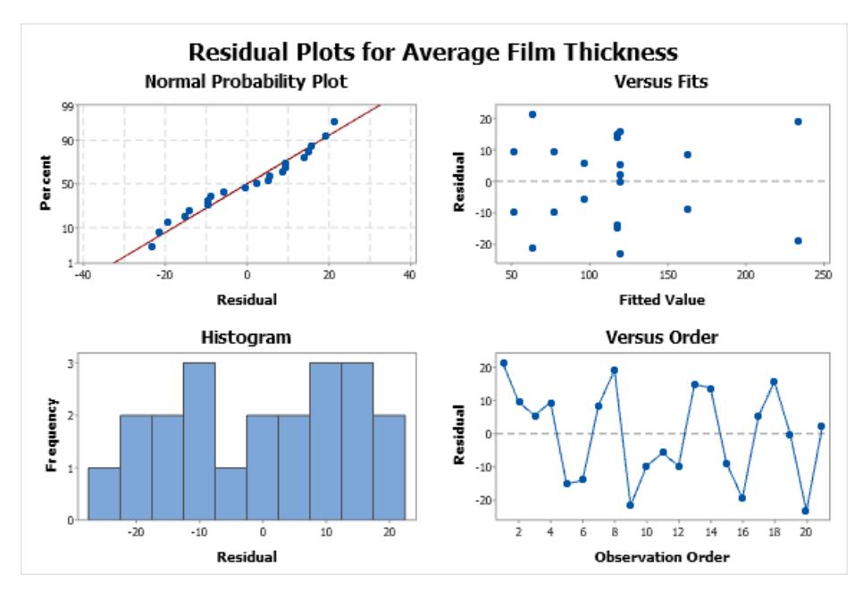
The residual plot of average film thickness.
In this Pareto chart, the standardized effects, represented by t-statistics, are employed to assess the null hypothesis, which posits that the effect is zero. The factors denoted as C, B, BC, ABC, and AC are depicted by bars in the chart, each crossing the reference line at 2.18. Notably, with the current model terms, these factors demonstrate statistical significance at the 0.05 level, indicating their substantive influence on the observed outcomes. Further analysis reveals the order of impact within the chosen range, with factors C, B, BC, ABC, and AC exhibiting progressively diminishing effects in the sequence C > B > BC > ABC > AC. This hierarchical arrangement underscores the differential contributions of each factor to the observed variance in the experimental outcomes, providing valuable insights into the underlying mechanisms governing the synthesis process.
According to the response optimizer function illustrated in Figure 4, the optimal conditions for achieving maximum average film thickness include an electric power of 100 W, a C2H2:H2 ration of 50:50, and a discharge time of 10 min. Under these optimized parameters, the resultant average film thickness was calculated as 51.13 nm. This finding highlights the efficacy of the response optimizer function in identifying the ideal combination of synthesis parameters to enhance the desired outcome. By systematically exploring the parameter space and optimizing the experimental conditions, researchers can effectively fine-tune the synthesis process to achieve desired film thickness values, thereby advancing the overall efficiency and effectiveness of graphene synthesis methodologies.
| Table 5 | Analysis of variance for average film thickness. | |||
|---|---|---|---|---|
| Source | DF | Adj SS | Adj MS | F-Value | P-Value |
|---|---|---|---|---|---|
| Model | 8 | 50295.9 | 6287.0 | 19.21 | 0.000 |
| Linear | 3 | 37200.6 | 12400.2 | 37.89 | 0.000 |
| Electric Power | 1 | 397.7 | 397.7 | 1.22 | 0.292 |
| Ratio | 1 | 7144.1 | 7144.1 | 21.83 | 0.001 |
| Discharge Time | 1 | 29658.9 | 29658.9 | 90.62 | 0.000 |
| Two-Way Interactions | 8756.7 | 2918.9 | 8.92 | 0.002 | |
| Electric Power*Ratio | 38.5 | 38.5 | 0.12 | 0.737 | |
| Electric Power*Discharge Time | 2652.5 | 2652.5 | 8.10 | 0.015 | |
| Ratio*Discharge Time | 1 | 6065.7 | 6065.7 | 18.53 | 0.001 |
| Three-Way Interactions | 1 | 4246.8 | 4246.8 | 12.98 | 0.004 |
| Electric Power*Ratio*Discharge Time | 1 | 4246.8 | 4246.8 | 12.98 | 0.004 |
| Curvature | 1 | 91.8 | 91.8 | 0.28 | 0.606 |
| Error | 12 | 3927.7 | 327.3 | ||
| Total | 20 | 54223.6 | |||
| R-sq = 92.76% | R-sq (adj) = 87.93% | ||||
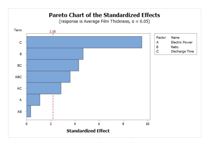
Pareto chart of the average film thickness.
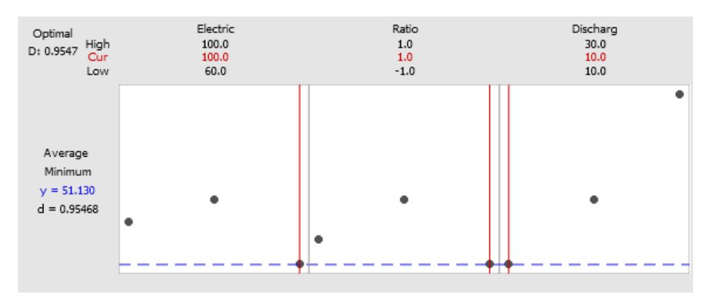
Optimal condition for the average film thickness.
Raman spectroscopy analysis of thin film composition.
Identification of Thin Film Composition using Raman Spectroscopy Analysis
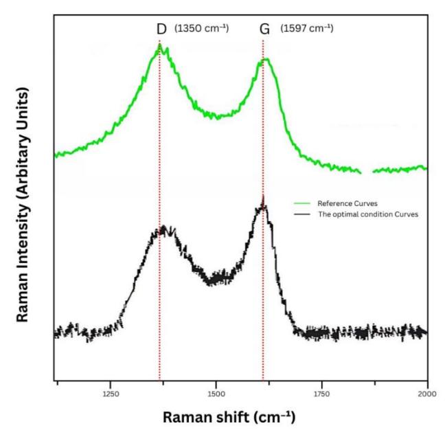
Raman spectroscopy was employed to investigate the composition and structure of the thin films synthesized during the experimental process. Figure 5 shows the Raman spectra, with a focus on the D and G peaks (Scardaci & Compagnini, 2021), which are commonly associated with carbon materials, and highlights the structural properties of the synthesized film. The D peak observed at 1,350 cm⁻¹ represents the breathing mode of k-point phonons in sp²-hybridized carbon atoms. This peak is typically indicative of structural defects or disorder within the graphene lattice, such as vacancies or grain boundaries. Meanwhile, the G peak positioned at 1,597 cm⁻¹ corresponds to the in-plane vibrational mode of sp² bonded carbon atoms, which is characteristic of graphitic materials. In the present study, the D/G intensity ratio provides insight into the disorder level and crystallinity of the synthesized graphene film. According to the research by Scardaci and Compagnini (2021) , a higher D/G ratio is typically associated with an increased degree of disorder or reduced graphene oxide (rGO) after laser scribing. In this study, the observed D/G ratio is crucial for understanding the extent of defects introduced during the plasma-enhanced chemical vapor deposition (PECVD) process. Under the optimal synthesis conditions (electric power of 100 W, acetylene-to-hydrogen ratio of 50:50, and discharge time of 10 minutes), the D/G ratio was significantly reduced, indicating improved structural quality of the graphene film with fewer defects. This contrasts with the reference sample, which exhibited a higher D/G ratio, suggesting a greater degree of disorder in its structure. Plasma treatment conditions for the sample include an electric power of 50 W and a base pressure of 2 × 10⁻² Torr. The D and G peaks in the spectrum were fitted to provide a clearer understanding of the film's composition and structural characteristics. Further comparison with Scardaci and Compagnini's findings reveals the relationship between synthesis conditions and the resulting graphene quality, suggesting that the plasma-enhanced process utilized in this work yields films with a moderate level of disorder compared to typical reduced graphene oxide (rGO) structures.
Discussion
In this section, we discuss the implications of our experimental findings, exploring the intricate relationships between the various synthesis parameters and the resulting properties of graphene films. By analyzing key factors such as electric power, gas ratios, and discharge time, we provide insights into the optimization of graphene synthesis using PECVD. Furthermore, we assess the correlation between film thickness and the D/G ratio, explore surface properties and wettability, and conduct a thorough morphological and structural analysis using Raman spectroscopy. Finally, we discuss the potential future directions and prospects for further research and applications of graphene-based materials.
The Effects of Process Parameters on Graphene Synthesis
Our experimental results both align with and extend previous findings, offering a comprehensive understanding of how various parameters influence graphene film properties. Consistent with research by Ma et al. (2019) and Phiri et al. (2018), we observed that increasing electric power leads to thicker graphene films. Higher power levels facilitate greater precursor decomposition and enhanced carbon atom deposition, corroborating the observations of Mehedi et al. (2020). This finding underscores the critical role of electric power in modulating film thickness. Specifically, films produced at 100 W were consistently thicker compared to those at 60 W, demonstrating a direct correlation between electric power and film thickness. Additionally, our results confirm that acetylene-rich environments contribute to thicker films compared to hydrogen-rich ratios, consistent with the study by Stephen et al. (2023) that highlights the superior deposition rates and film quality associated with higher acetylene concentrations. Our experiments showed that a 50:50 acetylene-to-hydrogen ratio resulted in a significant increase in film thickness compared to a 30:70 ratio, emphasizing the importance of gas composition in the synthesis process.
Furthermore, our study expands on existing knowledge by elucidating the effect of discharge time on film structure. Longer discharge times generally led to increased film thickness and enhanced structural properties, aligning with observations from prior research (Kalita et al., 2012) (Stephen & Hong, 2023). For instance, films deposited for 30 minutes exhibited notably greater thickness and uniformity compared to those deposited for only 10 minutes. This aspect of our study reveals the nuanced interplay between synthesis duration and film quality, offering new insights into the optimization of deposition processes. By integrating these findings, we provide a more detailed understanding of how process parameters affect graphene film synthesis, laying a foundation for further refinement and optimization of synthesis protocols. This comprehensive analysis highlights the importance of optimizing each parameter individually and in combination, advancing the field by elucidating the relationships between key experimental conditions and graphene film composition.
Film Thickness and D/G Ratio Analysis
The D/G ratio derived from Raman spectroscopy is a crucial metric for assessing the quality of graphene films because it reflects the level of disorder within the material. The results presented in Table 4 reveal that variations in synthesis parameters significantly impact the D/G ratio. Specifically, lower electric power (60 W) and a C₂H₂-to-H₂ ratio of 30:70 generally result in lower D/G ratios, indicating higher-quality graphene with fewer defects. This trend aligns with findings from previous studies, which suggest that lower power settings promote more uniform graphene growth and reduce the formation of structural defects (Li et al., 2016) (Wimalananda et al., 2017). Conversely, higher electric power (100 W) and a 50:50 gas ratio yield higher D/G ratios, which may be attributed to increased disorder or incomplete graphene formation due to the more aggressive conditions (Yang et al., 2019) (Kalita et al., 2012). Moreover, the effect of discharge time on the D/G ratio is notable. Extended discharge times (30 minutes) tend to increase the D/G ratio, reflecting higher levels of disorder or surface roughness. This contrasts with shorter discharge times (10 minutes) that typically result in lower D/G ratios and better film quality. This observation supports the notion that excessive discharge times exacerbate defects and disrupt the uniformity of graphene growth (Ma et al., 2017) (Phiri et al., 2018). Overall, optimizing the electric power, gas ratio, and discharge time is essential for controlling the D/G ratio and achieving highquality graphene films, as corroborated by both this study and the existing literature.
Surface Properties and Wettability
Our experimental findings resonate with and augment insights from previous studies, enriching our understanding of surface characteristics and their implications. Consistent with research by Iqbal et al. (2019), our study confirms the pivotal role of surface preparation and plasma treatment in modulating surface wettability. Specifically, our findings demonstrate that the dual-step cleaning regimen involving acetone and alcohol immersion, coupled with argon plasma treatment, effectively enhances surface cleanliness and promotes adhesion for subsequent graphene deposition, aligning with the observations of Song et al. (2021). Furthermore, our analysis of contact angle measurements underscores the importance of assessing surface wettability, as evidenced by the variations in contact angles observed under different experimental conditions. These results are consistent with the findings of Kruszelnicki et al. (2024) and Thomas et al. (2019). By integrating our results with the existing literature, our study provides a comprehensive understanding of surface properties and wettability dynamics, laying the groundwork for the informed design and optimization of graphene synthesis processes.
Morphological Analysis and Structural Analysis with Raman Spectroscopy
Our experimental outcomes are consistent with and complement findings from prior studies, enriching our comprehension of graphene morphology and structural characteristics. Consistent with research by Sui et al. (2017), our study confirms the utility of atomic force microscopy (AFM) in providing high-resolution images and detailed topographical information. Our results demonstrate the effectiveness of AFM in revealing surface morphology and topographical features [22], corroborating observations by Vasić et al. (2017) in [23]. Additionally, our analysis using Raman spectroscopy offers valuable insights into graphene film structure and purity, aligning with the findings of Marta et al. (2016) and Moreno-Bárcenas et al. (2018). The identification of diamond-like carbon (DLC) structures using Raman spectroscopy, as observed in our study, further underscores the versatility of this technique in characterizing different carbon structures, consistent with previous research [24,25]. By integrating our findings with the existing literature, our study provides a comprehensive understanding of graphene morphology and structural analysis, facilitating informed decision-making in graphene synthesis and application development.
Future Directions and Prospects
Our experimental outcomes, congruent with prior investigations, illuminate potential avenues for advancing graphene synthesis and applications. Building upon the insights garnered from studies by Kalita et al. (2012) and Zhang et al. (2022), our findings underscore the need for continued exploration of novel synthesis techniques and parameter optimizations to enhance graphene film properties. Drawing from the observations of Liu et al. (2017), future research endeavors could elucidate the underlying mechanisms governing the interplay between process parameters and film characteristics, facilitating the development of predictive models for synthesis outcomes. Additionally, insights gleaned from Raman spectroscopy analysis, as highlighted by Dasari et al. (2017) and Wahab et al. (2024), suggest paths for exploring alternative carbon structures and their functional properties, thereby opening avenues for tailored graphene applications in diverse fields. By integrating our findings with the existing literature, this study lays the groundwork for future investigations aimed at refining synthesis protocols, uncovering new material properties, and advancing the utilization of graphene in various technological applications.
Conclusion
In conclusion, this study showcases the effectiveness of PECVD in synthesizing graphene films with optimized properties. By systematically varying key parameters such as electric power (ranging from 60 to 100 W), the acetylene-to-hydrogen ratio (varying from 30:70 to 50:50), and discharge time (ranging from 10 to 30 min), we identified optimal conditions that resulted in significant improvements in film thickness and structural integrity. The film thickness varied between 41.51 and 253.80 nanometers, and the D/G ratio, a key indicator of film quality, fluctuated accordingly. Lower D/G ratios, observed with lower electric power and specific gas ratios, suggest higher-quality graphene with fewer defects. Conversely, higher D/G ratios, associated with higher power settings and longer discharge times, indicated increased disorder. Our analyses, including atomic force microscopy and Raman spectroscopy, provided critical insights into the impact of these synthesis parameters. Assessments of surface properties and wettability underscored the role of surface interactions in determining the applicability of graphene films across various fields. The optimized synthesis conditions established in this study offer a solid foundation for further exploration and the development of graphene-based materials, promising advancements in electronics, energy storage, and biomedical engineering. By integrating these insights and numerical findings, this research contributes significantly to the ongoing pursuit of technological innovation and scientific progress.
Acknowledgement
We extend our sincere gratitude to Natwara Kanthikul and Lanlalit Acheewanunt for their invaluable assistance in collecting the experimental results, which significantly contributed to the success of this research. We also acknowledge the Department of Industrial Engineering, Faculty of Engineering, Chiang Mai University, for providing the necessary facilities and experimental equipment, which enabled the completion of this study.
Conflicts of Interest
All authors should disclose in their manuscript any financial or other substantive conflict of interest that might be construed to influence the results or interpretation of their manuscript.