
1 Introduction
Convolutional encoding is often preferred among error correction coding methods in digital communications because of its high coding gains [1]. For its corresponding decoding scheme, the Viterbi decoding algorithm is the most popular method [2]. High coding gains with low error probability and high throughput processing are extensively needed for high-speed applications [3]. Hence, many researches have been conducted to explore the Viterbi decoding algorithm, especially for implementation in VLSI. Principally, single complete convolutional error correction consists of three main processes, i.e. convolutional encoding, transmission error disturbance and Viterbi decoding. The original data are convoluted by using a specific convolution calculation in order to produce the codewords. Every single codeword represents the original data and its redundant bits. Hence, if errors occur in the middle of data
transmission, the receiver will be able to reconstruct the correct data by using the Viterbi decoding algorithm.
There are many publications about Viterbi decoder implementation in VLSI. Habib, et al. [2] discuss a VLSI design space exploration for a hard-decision Viterbi decoder. They describe any explorations that can be considered in designing a Viterbi decoder. Jinjin He, et al. [4] have proposed a low-power and high-speed Viterbi decoder using the T-algorithm for trellis coded modulation (TCM). A low-power design is important because a Viterbi decoder has high power consumption in TCM systems [5]. Low-power issues are quite popular, hence many researches on this topic have been presented (e.g. [4-8]). Besides power consumption, researches have been done on speed performance [9] and area efficiency (e.g. [10-14]). Furthermore, a comparison of Viterbi designs [15] and a configurable Viterbi decoder design [16] have been presented as well.
The Viterbi decoding algorithm is usually implemented in a hardware circuit, since its process needs fast computation. In order to use its error correction capability in various real-time applications (e.g. mobile communication, software defined radio, etc.), Viterbi decoders are highly considered to be integrated in a hardware-software (HW-SW) co-design system, such as Systemon-Chip (SoC). Nowadays, SoC technology has driven many developments in electronic devices [17-18] because it provides powerful and flexible solutions for real-time applications. Integrating the Viterbi decoder into such systems is highly demanding. In order to get full benefit of various real-time error correction applications, a configurable design for the Viterbi decoder is needed. Thus, the application scheme can define how the Viterbi decoder should respond using only soft programming. Meanwhile, the error correction process can be done quickly, since it proceeds in the hardware circuit. This is what makes configurability in the Viterbi decoder design important.
Our literature study showed that most researches discuss speed performance, low power consumption and area efficiency issues. These topics have been explored and discussed extensively because of their importance. Unfortunately, we found that only few researches have explored and discussed configurable and low-complexity designs. The main challenge in designing a configurable architecture is to accommodate several scenarios of trace-back and multiple constraint lengths in the hardware circuit. This may be the reason only few configurable designs have been reported.
Hence, in this research, we designed a configurable and low-complexity VLSI architecture for a hard-decision Viterbi decoding algorithm. The proposed configurable architecture means that the design trace-back implementation can be changed without any major modifications in the RTL code, but only by changing the predefined number of trace-back parameters. Thus, the architecture has to be as generic as possible. Meanwhile, the proposed lowcomplexity architecture means that the design only consists of simple logical operations. Thus, the architecture has to be optimized at the logic operation level. Furthermore, we chose the hard-decision category because of its simplicity for the first fundamental research. A hard-decision design means that the Viterbi decoder only uses two levels of decision, high '1' and low '0' [19]. These are our research goals.
In this research, three main design steps were involved. The first one was to extract the fundamental processing element (PE) from the Viterbi algorithm. This extraction was conducted to optimize the three main units in the Viterbi decoder architecture: the branch metric unit (BMU), path metric unit (PMU), and survivor memory unit (SMU). The second step was to design a conditional adapter unit for the purpose of configurability. The last step was to incorporate the entire architecture in a generic structure.
This paper is divided in a number of sections. The first section is an introduction about the research background and related past researches. The second section contains a brief explanation of the convolutional error correction methodology. This is followed by the proposed design, results and analysis sections. The last three sections are concluding remarks, nomenclature and references, respectively.
2 Fundamental Concepts
2.1 Overview
The fundamental mechanism in convolutional error correction consists of three main elements: convolutional encoding, transmission, and Viterbi decoding, as illustrated in Figure 1. In the convolutional encoding process, the encoder will produce codewords (c) from the original data (dO). A codeword represents the original data and its redundant bits. These codewords will be sent from a transmitter to a receiver through a transmission channel. In the transmission channel, the data may be changed because of error disturbance. Thus, the data received (e) at the receiver may contain errors. These received data (e) have to be checked and processed in the Viterbi decoder in order to obtain the correct data (dR), because the Viterbi decoder contains an error correction algorithm that can reconstruct the original data.
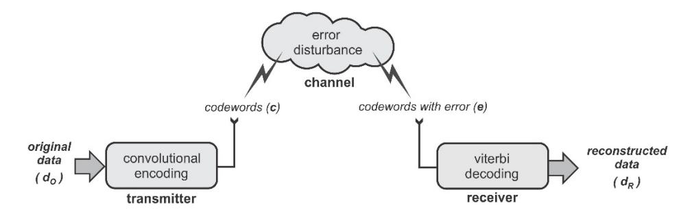
Figure 1 Block diagram of convolutional error correction mechanism.
2.2 Convolution Encoder
The convolution encoder is the first element of the convolutional error correction method. It encodes the original data (dO) into codewords (c). The convolutional encoder has several important terms regarding its computation. They are called code rate (R), constraint length (K), number of states (S), original input data (dO), and encoded data or codewords (c). Constraint length K represents the length of the convolutional encoder process. It is defined by the number of shift-registers used in the process, plus one [2]. Figure 2 shows an illustration of convolutional encoding used in our research. We can also formulate the polynomial codeword generator, as shown in Eqs. (1) and (2). The number of states S of the convolutional encoder is a function of the original input data bits (dO-bits) and the constraint length K [20]. Its formulation is presented in Eq.(3). Meanwhile, code rate R represents the ratio between number of original input bits (dO-bits) and number of encoded bits (c-bits). Its formulation is presented in Eq.(4). In this research, we have chosen K = 4, R = 1/2, and dO-bits = 1 bit. Thus, there are 3 shift-registers and 2 bits of code-word c.
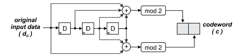
Figure 2 Block diagram of convolutional encoding scheme (K = 4, R = 1/2).
\[G^{(1)} = 1 + D + D^2 + D^3 \tag{1}\]
\[G^{(2)} = 1 + D^2 + D^3 \tag{2}\]
\[S = 2^{\{d_{O-bitwidth}(K-1)\}}; d_O \text{ bit-width}\] (3)
\[R = \frac{d_{O-bitwidth}}{c_{bitwidth}} \qquad ; d_O \text{ and } c \text{ bit-width}\] (4)
2.3 Viterbi Decoder
In the Viterbi decoding process there are specific decoding operations based on the corresponding computation in the convolutional encoder. There are three main elements in the Viterbi decoder, i.e.: the branch metric unit (BMU), path metric unit (PMU), and survivor memory unit (SMU). BMU is used for calculating the code distance between codewords \(\boldsymbol{c}\) and comparator \(\boldsymbol{r}\) [21], PMU is used for accumulating the distance from BMU for every stage, and SMU is used for storing the bit decision produced by PMU [2]. A generic block diagram for the Viterbi decoder architecture is shown in Figure. 3. BMU, PMU, and SMU are sequentially connected to decode the given codewords.

Figure 3 Generic block diagram for Viterbi decoder.
Figures 4 and 5 show the finite state machine (FSM) and trellis network that represent the Viterbi decoding process, which is formulated from the corresponding convolutional encoding in Figure 2. This indicates the state values S, predictors i, and comparator r. State values S are represented in 3-bit binary, which mean there are 8 states of convolutional encoding. This is obtained from calculation \(S = 2^{\{d_{O-bitwidth}(K-1)\}} = 2^{\{1(4-1)\}} = 8\) states. During computation, the predictors are involved as prediction values for determining the right reconstructed bit. The solid-arrow line represents the predictor i = 0, while the dashed-arrow line represents the predictor i = 1. Lastly, the comparator values are written near the arrow line. The comparator values are compared to the codewords in order to determine the Hamming distance, which represents the number of errors. For this operation, compare-select-add (CSA) is used, as shown in Figure 6. The CSA method was chosen because of its efficient implementation. Comparison is done first before selection and addition, hence we only compute addition once for each selected survivor \((\theta)\). We also optimize the process through bit-level optimization. Bit-level optimization is suitable in VLSI, as was found in past researches (e.g. [22]-[24]).
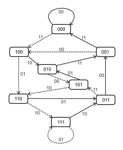
Figure 4 FSM of Viterbi decoding algorithm.
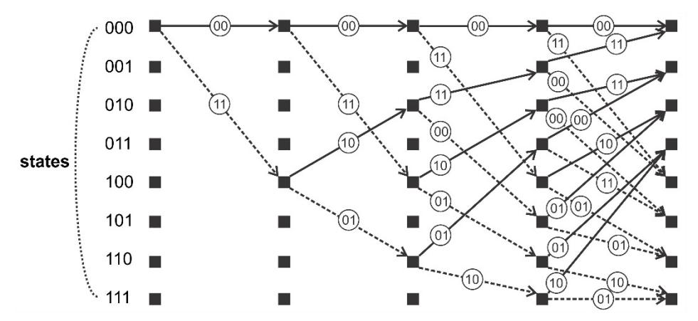
Figure 5 Trellis of Viterbi decoder for trace-back N = 4.
As a practical example, Figures 4 and 5 show that the computational state begins at current state P = "000". When the received codeword e comes in, the Viterbi decoder involves the predictors i = '0' and i = '1' into the process. If predictor i = '0', then next state Q = "000" and comparator r is "00". Meanwhile, if predictor i = '1', then next state Q = "100" and comparator value r is "11". For every prediction process, the received codeword e is compared to the corresponding comparator value r. Each comparator value r examines each
received codeword e to determine the Hamming distance or weight (w). Survivor θ with the minimum Hamming distance w is considered to be the reconstructed data (dR).
Figure 6 Design space of Viterbi decoder for VLSI [2].
3 Research Methodology
Three design approaches were involved in this research. The first approach was designing an efficient processing element (PE). This was achieved by optimizing the three main units in the Viterbi decoder (i.e. BMU, PMU and SMU). BMU is used to calculate the code distance between codewords c and comparator r, thus efficient logic operation and addition are required. PMU accumulates the calculated distances from BMU, while SMU stores the bit decision produced by PMU. Because the data from PMU are stored in SMU, we can optimize these two units together. Moreover, BMU, PMU and SMU can be designed in a parallel instead of a sequential structure. Thus, operation delay can be minimized. The second approach was designing a conditional adapter unit for the purpose of configurability, based on predefined configurability parameters. This manages bit-width consumption, counter, and iteration steps based on the trace-back parameters. The final approach was designing the entire architecture in a generic structure, thus enabling the architecture to be extended and pipelined easily.
4 Proposed Architecture
4.1 Efficient Processing Element (PE)
The processing element (PE) is responsible for all logic operations conducted in the Viterbi decoder. In order to achieve the low-complexity target, PE has to be designed as simple as possible. Each PE has two main computations: compareselect-add (CSA) and data storage operations. CSA operation determines the survivor, while the data storage operation updates and keeps the survivor information (i.e. current reconstructed data and their Hamming distances). Figure 7 shows an illustration of these operations in the PE. The solid arrow line represents the predictor '0', while the dashed arrow line represents the predictor '1'.
Figure 7 Illustration of a single processing element (PE).
We optimize the BMU, PMU, and SMU concepts to result in a single processing element (PE). In every single PE, the Hamming distance or weight w is calculated with pseudoformula in Eqs. (5)-(6) by using only bitwise XOR logic operation ⊕ and addition (+). Distance w is calculated from the difference value between error codeword e with comparator r. Hence, bitwise XOR operation is needed, followed by addition. The bitwise XOR logical operation and addition processes are shown in Eqs. (5) and (6) respectively, while the full calculation is shown in Eq. (7).
\[b_{m,n} = r_{m,n} \oplus e_{m,n} \tag{5}\]
\[W_{m,n} = b_{m,n}[1] + b_{m,n}[0]\] (6)
\[W_{m,n} = \left(r_{m,n}[1] \oplus e_{m,n}[1]\right) + \left(r_{m,n}[0] \oplus e_{m,n}[0]\right) \tag{7}\]
From Eqs. (5)-(7), we can derive the total Hamming distance (W) in the single trellis survivor (Wm), which can be obtained with pseudo-formula in Eq.(8).
\[W_{m} = \sum_{n=0}^{N-1} w_{m,n} \tag{8}\]
State \(Q_{m,n}\) has parameters (m,n), which indicate trellis step (m) and trace-back step (n). Trellis step means the step number of the survivor chain. Hence, after a trellis survivor passes a PE, the trellis step will be doubled because of two probabilities of predictor i. Trace-back step n means the step number of the trace that occurs in the processing. Complete trace-back step n is equal to traceback number N. Next state value Q depends on predictor \(i = \{0,1\}\) and previous state P. The next survivor is written as \(\theta_{m,n}\). This is constructed from concatenation of previous data \(\theta_{m,n-1}\) and estimated predictor i. The last survivors of \(\theta_{m,n}\) at the end of trace-back are considered to be the reconstructed data \(d_R\) by comparing them with each other to get the smallest value of total distance W. Pseudo-formula in Eq.(9) shows how the next state \(Q_{m,n+1}\) is determined. Next state \(Q_{m,n+1}\) is obtained by concatenating predictor i with 2-MSB from previous state \(P_{m,n}\). Pseudo-formula in Eq.(10) shows how the survivor is reconstructed. Survivor data \(\theta_{m,n}\) are obtained by concatenating previous survivor \(\theta_{m,n-1}\) with corresponding predictor i. Lastly, survivor \(\theta\) with minimum weight w is considered to be the reconstructed data \(d_R\), as stated in Eq.(11).
\[Q_{m,n+1} = \begin{cases} i = 0 \to Q_{(m,n+1)} = \{'0', P_{m,n}[2:1]\} \\ i = 1 \to Q_{(m,n+1)} = \{'1', P_{m,n}[2:1]\} \end{cases}\] \[(9)\]
\[\theta_{m,n} = \left\{ \theta_{m,n-1}, i_{m,n} \right\} \tag{10}\]
\[d_R = \min\{\theta_0, \theta_1, \theta_2, \dots, \theta_{s-1}\}\tag{11}\]
In the Viterbi decoder core design there are 8 PEs representing 8 states. We can extract the trellis network connections in Figure 5 to create simple network connections as shown in Figure 8. These structures can be called butterfly pairs [25]. We can see that each state has a structure identical to the PE from Figure 7. Because of its identical structure, we only need to create a single optimized PE and copy it eight times to represent \(S_0\) - \(S_7\). We also can see that each PE exactly has 2-way directional input and output (I/O). Hence, each PE has to accommodate the following datapaths.
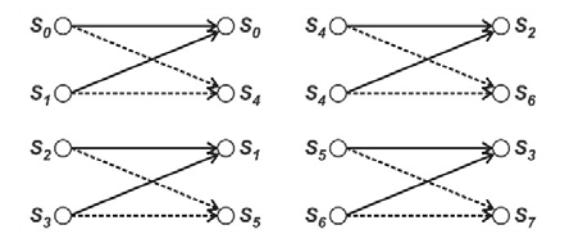
Figure 8 Extracted Viterbi network connections.
After defining the PE's I/O structure and extracting the trellis network connections, the detailed PE architecture can be designed. Figure 9 shows the detailed architecture for a single PE. We can see that BMU, PMU and SMU are not separated distinctively. They are combined and optimized to become one single PE. There are only bitwise XOR logic, addition, concatenation, multiplexing, and shift-register operations. This shows that the PE architecture is low-complexity. Moreover, this architecture is designed to form a parallel structure, thus it is easy to pipeline. If we want to decrease the operational delay, we can examine the worst-case delay path and insert the pipeline there.
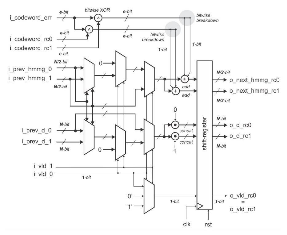
Figure 9 Detailed architecture for single PE.
4.2 Core Architecture
The core of the Viterbi decoder is constructed from eight PEs, 8 multiplexers and a single comparator, as illustrated in Figure 10. This receives data from the multiplexers and the broadcasted error codewords. This means that all PEs accept the same codewords. The multiplexers select which data from the previous process are passed to the PEs. Meanwhile, the comparator selects the last survivor with minimum distance W as reconstructed data dR. By using this generic architecture, the design can be easily pipelined and extended for further purposes.
Figure 10 Core architecture of Viterbi decoder.
4.3 Conditional Adapter
In order to make a configurable design for any predefined number of tracebacks, we need to design a conditional adapter. This consists of a finite-input unit and a multiplexer block. The conditional adapter is responsible for receiving and managing the e-bit data (i.e. error codeword) and deliver them to the Viterbi core in codeword size (c-bit). In detail, the finite-input unit manages the size of the input and stored data, while the multiplexer block manages the size of the data that are transferred to the Viterbi core. Thus, in order to synchronize the process in the conditional adapter and the Viterbi core, there is a control signal, which is produced by the finite-input unit to control the process in the multiplexer and the Viterbi core. A detailed illustration of the conditional adapter unit is presented in Figure 11. In the finite-input unit, there are two
functional sections, i.e. the data buffers and the finite-state controller. The data buffers are established by the finite number of registers. The number of registers are determined by the error-codeword bit-width (e-bits). Meanwhile, the finitestate controller is responsible for controlling the flow of the decoding process. This finite-state controller selects the buffered data to be passed into the Viterbi core through a multiplexing mechanism and gives a status signal in order to control the decoding process.
Figure 11 Conditional adapter architecture.
4.4 Top Level Integration
Integrating the conditional adapter and the Viterbi core results in the whole decoder design. A top level illustration of the Viterbi decoder is presented in Figure 12. From this illustration, we can see that the proposed architecture is actually in a simple generic form. The datapath bit-width and trace-back parameters can be adjusted for specific needs and are set in the pre-synthesis process.
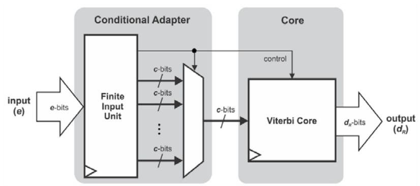
Figure 12 Detailed top level design of Viterbi decoder.
5 Results and Analysis
5.1 Functional Simulation
Functional simulation was done using waveform analyzer software. The design configurations were tested for four trace-back scenarios (i.e. N = 8, N = 16, N = 32 and N = 64). A testbench provided raw test data (original data) and triggered the simulation. We could observe the convolutional encoding, transmission error disturbance and decoding processes. Figures 13-16 show the results. The first process arrow indicates the convolutional encoding process, the second one indicates the transmission error disturbance process and the last one indicates the Viterbi decoding process. The design with trace-back N = 8 needed 10 clock cycles latency, while the designs with trace-back N = 16, N = 32, and N = 64 needed 18, 34, and 66 clock cycles latency, respectively. These results show that the proposed design only needs N + 2 clock cycles latency to produce valid data.
Figure 13 Waveform simulation for trace-back N = 8.
Figure 14 Waveform simulation for trace-back N = 16.
Figure 15 Waveform simulation for trace-back N = 32.
Figure 16 Waveform simulation for trace-back N = 64.
5.2 Synthesis Results
Design synthesis scenarios were conducted for N = 8, N = 16, N = 32 and N = 64 trace-back designs in FPGA Altera Cyclone II EP2C35F672C6 and Xilinx Virtex 6 XC6VCX75T. There are two major categories of synthesis evaluation: area occupation and computational speed. Both are presented in Table 1. From the synthesis reports, we can see that if a higher number of tracebacks is chosen, the area occupation increases because if the trace-back number is higher, the computation size will be higher too. The hardware architecture needs to accommodate the possibility of the calculated value. This condition affects the performance speed. The speed of calculation decreases along with the increase of the trace-back number. Overall, the synthesis results delivered promising area occupation and performance speed values.
| Trace Back (N) | Clock Cycles Latency | Area (Logic Utilization) | Speed (MHz) | ||
|---|---|---|---|---|---|
| 8 | 10 | 627 LEs 1197 LEs 2238 LEs | 148.70 | ||
| Altera | 16 | 18 | 120.15 | ||
| Cyclone II | 32 | 34 | 92.20 | ||
| 64 | 66 | 4325 LEs | 69.18 | ||
| 8 | 10 | 537 LUTs | 139 Regs | 312.36 | |
| Xilinx | 16 | 18 | 1129 LUTs | 287 Regs | 254.44 |
| Virtex 6 | 32 | 34 | 2305 LUTs | 576 Regs | 228.29 |
| 64 | 66 | 4521 LUTs | 1160 Regs | 157.15 | |
Table 1 Synthesis results.
Nomenclature LEs: Logic Elements LUTs: Look-up Tables Regs: Registers
5.3 Benchmarks
Benchmarks with other works are not easy to establish, because publications about a Viterbi decoder with K = 4 and R = 1/2 are relatively hard to find. In several cases, the existing publications cannot be compared to the proposed design directly because each publication usually has a specific application issue. Fortunately, we managed to find a publication which uses the same parameters. The benchmarks derived from this work are presented in Table 2. We can see that our proposed design has a smaller latency, smaller area occupation, and good performance speed. Although its performance speed was slower than the design [26] in Altera Cyclone II, its area occupation and latency were smaller. For Xilinx Virtex 6 implementation, our proposed design was better in all investigated aspects (i.e. latency, area occupation, and performance speed). Moreover, the design time of the proposed method only needed around one day of mathematical works for operational optimization and 1-2 days of Hardware Description Language (HDL) coding and implementation. This is quite fast for research development.
Works K R Trace Back Clock Cycles Latency Altera Cyclone II Xilinx Virtex 6 Area (LEs) Speed (MHz) Area (LUTs) Speed (MHz) Paper [26] 4 1/2 32 35 3572 132.73 3519 179.46 Proposed 4 1/2 32 34 2238 92.20 2305 228.29
Table 2 Design benchmarks.
5.4 Future Research
The proposed method offers two possibilities that can be further explored in the future. The first one is designing possible extensions for specific applications. For example, if we want to increase the performance speed and throughput, we can use pipelining techniques. If we observe Figures 9 and 10, there are opportunities to insert pipelines into the design. There is a sequence of logical operations (i.e. XOR and addition) that can be separated by a pipeline in order to increase the processing speed and throughput. Thus, we need to adjust the operational finite-state machine (FSM) to implement that strategy. The second possibility is implementing the proposed technique for a soft-decision Viterbi decoder. A soft-decision approach is necessary in particular cases. Hence, future research on this topic is important.
6 Conclusions
A configurable and low-complexity VLSI architecture for a hard-decision Viterbi decoder were presented in this paper. The design can do error correction and produce valid reconstructed data. The design can be configured for any predefined number of trace-backs. This is achieved by changing the trace-back parameter value. It only needs N + 2 clock cycles latency to complete the process, with N is the number of trace-backs. Its configurability function was validated for N = 8, N = 16, N = 32 and N = 64. The design was also synthesized and evaluated in both Xilinx and Altera FPGA target boards for area consumption and speed performance. The proposed design produced promising synthesis results. There are two main possibilities this method offers that can be explored in the future: designing possible extensions for specific applications and implementing the proposed technique for a soft-decision Viterbi decoder.
Nomenclature
dO = original data
c = codewords / encoded data / transmitted data
e = error codeword / received data
dR = reconstructed data S = number of states
Sx = state x
K = constraint length
R = code ratio m = trellis number n = trace-back number P = PE current state Q = PE next state
Pm,n = (m,n)-specified state Qm,n = (m,n)-specified state
i = predictor / prediction value r = codeword comparator w = Hamming distance / weight
\(w_{m,n} = (m,n)\)-specified Hamming distance / weight
W = total Hamming distance / weight
\(W_m = (m)\)-specified total Hamming distance / weight
\(\theta\) = survivor
\(\theta_{m,n} = (m,n)\)-specified survivor