
1 Introduction
OFDMA-based 4G and 5G technologies provide high-throughput broadband wireless communication. These technologies employ complex multi-carrier signal processing to meet high throughput requirements. On the other hand, because of the large number of target applications for mobile and portable devices, data processing management is a crucial aspect to achieve low resource utilization by the OFDMA system. Furthermore, it also opens the possibility to reduce the power consumption level. To overcome these challenges, OFDMA processing implementation in system-on-chip (SoC) technology is needed. The main reason is that SoC technology can support resource usage management, which is crucial for performance and power consumption. Moreover, SoC technology can also be used for flexible purposes of applications. These benefits
currently make SoC technology popular as a solution for many different electronic applications [1,2]. Several variations of SoC techniques have been introduced, such as multiprocessor SoC (MPSoC) for parallel processing [3], multi-SoC for task partitioning [4], hybrid multi-SoC (H-MSoC) for highly flexible systems in application and task partitioning [1], etc.
MPSoC technology is considered a unique branch of computer architecture evolution since it has real-time low-power multitasking as a feature [3]. Considering this fact, we chose to design an OFDMA system on a single MPSoC platform and separate its implementation into hardware and software. The main target was to minimize the OFDMA processing hardware on a heterogeneous MPSoC platform, because minimizing the processing hardware leads to low-cost implementation and possibly also to low-power consumption while maintaining parallel processing performance. Four architectural concepts are proposed to implement this OFDMA MPSoC design.
The first concept is to overcome the computationally intensive signal processing of the OFDMA physical layer. We implemented the computation as an application specific integrated circuit (ASIC) module. Furthermore, parallel processing and pipeline architecture approaches are used at this level to maintain a low system frequency. By keeping the clock frequency low, the power consumption is expected to be low as well. The second concept is to implement the medium access control (MAC) and network layers in software, running on MPSoC processors because of their complex and dynamic data processing requirements. Software-based computation is slower than hardwarebased computation [5], thus to achieve high throughput, the MAC processor needs to work at a higher frequency than the physical layer. Therefore, the third concept is to propose a heterogeneous clocking system through multi-bus MPSoC. This is used to separate the physical layer ASIC from the data link layer processor, where each processor is working at its own clock frequency. Moreover, the data link can be implemented using a multi-core processor to reduce the clock frequency while keeping the same throughput rate.
To make the MPSoC system works properly and efficiently, a shared-memory mechanism is needed. Several shared-memory mechanisms can be found in the literature, such as [6-9]. For example, Greiner, et al. [6] proposed the Multi-Writer Multi-Reader (MWMR) communication middleware mechanism and Ahmed, et al. [5] proposed the CARER algorithm. From the literature, most of the proposed techniques have shared memory in a single-bus MPSoC architecture, which unfortunately is not suitable for our multi-bus architecture. A multi-bus architecture is usually built according to specific application needs. Hence, the mechanism needed to handle such specific needs varies based on many considerations (e.g., energy-efficiency, memory access, etc.) that correspond to the application. In such cases it is quite difficult to compare one mechanism to another. Since our case can hardly be found in the literature, we needed to specially design a mechanism to overcome this challenge. This led us to the use of inter-processor communication (IPC) as the last proposed concept.
Actually, the general IPC concept comes in various forms at the software level, for example in the operating system (OS) layer. We exploited the general IPC concept to build a custom and specific IPC table as a memory map of processors and peripherals that can accommodate multi-bus architecture. Using this proposed global table, each processor can freely access data from the other processors' memory or peripherals. This feature provides flexibility and efficiency in memory and data access between processors inside the system. This feature also makes it easy for the programmer to implement the code in each processor since each processor can work independently. Moreover, the number of processors or peripherals is not limited. Therefore, the proposed system is scalable to larger numbers of processors and larger computational power requirements.
This article is organized into several sections. Section 1 is the introduction, which briefly describes the research background and the proposed methodology. Section 2 explains the proposed MPSoC architecture, followed by a detailed explanation of the IPC architecture, while its mechanism is discussed in Section 3. This is followed by explanations of processor resource allocation, the network layer and FPGA implementation in three consecutive sections. System verification and the results thereof are provided and discussed in Section 7. This paper finishes with concluding remarks in Section 8.
2 Proposed MPSoC Architecture
The complete system architecture for the proposed MPSoC is illustrated in Figure 1. The system comprises two RISC based processing units, Processor-0 (RISC0) and Processor-1 (RISC1). RISC1 is allocated for the physical layer (PHY) function and RISC0 is allocated for the data link layer function. Two independent AHB-based high-speed buses are used, namely AHB0 and AHB1. Both buses work at heterogeneous clock frequencies. AHB0 works at a clock frequency of 40 MHz, while AHB1 works at a clock frequency of 80 MHz. The data interconnection between both buses is established through two AHB bridges.
AHB0 interconnects the main processing units, i.e. the physical layer module (PHY), the dual-core processors (RISC0 and RISC1), the direct memory access (DMA) master controller, the RF module, etc. AHB0 works at the same clock frequency as the RISC processors. AHB1 interconnects the system memories, i.e. the shared memory, the boot code, and other peripheral memories. Although the processors work at a lower frequency, the program memory is set to 80 MHz to maximize performance. Thus, AHB1's clock speed is increased to 80 MHz. The bus clock speed is made configurable for multiplications of 40 MHz. A higher frequency will increase the processing speed and the power consumption. Therefore, the optimum clock frequency will be decided based on the target implementation and data throughput.
Both AHB0 and AHB1 have their own bus arbiter, ARB0 and ARB1, which has the function to select the active slave at a particular time slot. The DMA master is used to transfer data between peripherals. Four DMA channels are used to support four types of data transfer, namely memory-to-register, register-tomemory, register-to-register, and memory-to-memory. The external interface, i.e. Ethernet, is connected through an Ethernet controller. The shared memory has the function to store the program and to process data for the connected system processors (RISC0 and RISC1). The shared memory (Shared RAM) is implemented using SDRAM. Each processor has a different memory allocation inside Shared RAM.
The APB bus is a low-speed bus that is used to interconnect low-speed peripherals for the baseband function, i.e. the DMA slave controller, SPI, timer, GPIO and UART. An AHB-APB bridge is used to establish the connection between the modules in the AHB bus and the APB bus. For the implementation, two LEON3 SPARC V8 32-bit processors are used as the main processors (RISC0 and RISC1). Gaisler's Library IPs (GRLIB) and an Advanced Microcontroller Bus Architecture (AMBA) bus system are utilized as well [10].
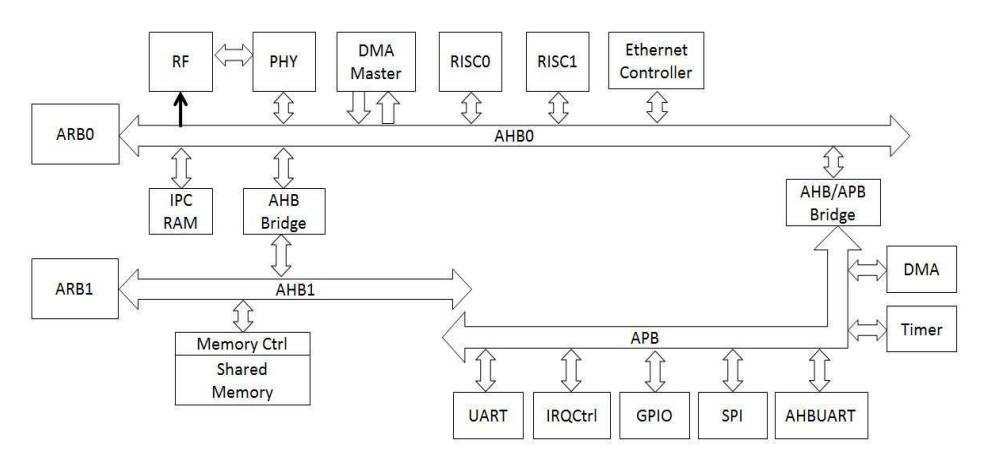
Figure 1 Proposed MPSoC architecture.
3 Inter-Processor Communication (IPC)
3.1 Architecture and Mechanism
Flexibility and efficiency of sharing data between processors are the most important characteristics of the MPSoC architecture. We propose an architecture and shared-memory mechanism that are flexible, efficient, and feasible to program. The data-sharing mechanism between the two processors (RISC0 and RISC1) was built using Shared RAM. Each processor has three allocated memories and a dedicated memory allocation inside Shared RAM, as illustrated in Figure 2. Inside the allocated memory address, each processor can freely allocate memory for its purpose. In Figure 2, mem0, mem1, and mem2 are allocated by RISC0 and mem3, mem4, and mem5 are allocated by RISC1. For instance, to support the PHY function, these memories can be used by RISC1 for data, transmitter (TX) buffer and receiver (RX) buffer. Each processor has a pointer to its allocated memory (i.e. *mem0, *mem1, *mem2).
If a processor wants to share its data with another processor, it has to pass the pointer of its allocated memory to the other processor. To pass this information, FIFOs are provided inside the inter-processor communication (IPC) RAM. Therefore, the other processor will have a complete set of memory pointers inside its IPC RAM, which it has the authority to access. Using these pointers, each processor can freely access all memories inside the Shared RAM. Using this mechanism, the proposed architecture can provide two types of data transfer between processors, memory pointers (IPC RAM) and data (Shared RAM).
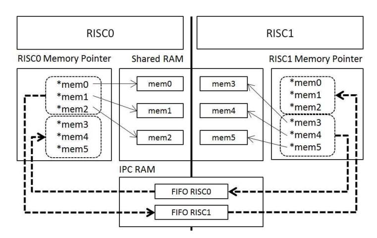
Figure 2 Proposed data-sharing mechanism using IPC.
The FIFO is provided to enable sending and receiving data between processors. Each processor has a dedicated FIFO inside its IPC RAM (i.e. IPC FIFO).
Therefore, the number of IPC FIFO is the same as the number of processors. The IPC FIFO works as the mailbox of each processor. If another processor wants to send data, it only has to write the data to the IPC FIFO of the designated processor. After the data have been written, the designated processor will be notified by an interrupt. The amount of data that can be transferred between processors is relatively small as it is limited by the size of IPC RAM. Hence, this type of communication is only used to send shared data information inside Shared RAM. After the Shared RAM information is received by the designated processor, it can start sharing the real data using Shared RAM instead of IPC RAM. Thus, Shared RAM is designed to have a larger capacity than IPC RAM. IPC RAM also can be used to transfer small amounts of data that require immediate action.
The real data shared between processors are stored inside Shared RAM. The size of memory allocation is free for each processor depending on need. However, it must be guaranteed that there will be no overlapping data. Each type of shared data must have a format known by the other processors and be defined as a data packet. The format must have a header or flag bit. This flag bit indicates that the data have been written or read, because only updated data will be read, and only empty allocations will be updated with new data. Therefore, to make sure the updated data can be read, the other processor should pool the header for information.
3.2 The IPC Sequence
To provide data sharing between processors, a sequence of processes must be executed by all processors. In this sequence, one processor will act as a master that controls the sequence. In the boot sequence, processor allocation memory reference data are sent through IPC RAM. The designated processor must provide space to store the references that are implemented with pointers. After each processor has obtained the references from the other processors, the communication between the processors can be performed through writing and reading those references. The IPC sequence is shown in Figure 3.
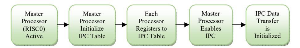
Figure 3 The IPC sequence.
At the start, only the assigned master processor is active, while the other processors and peripherals are halted. Hence, at this point only the master
processor can access the bus. In the proposed MPSoC system, we assign RISC0 as the master processor. As a consequence, RISC0 will occupy all buses and has the privilege to create content inside IPC RAM. At this stage, the master processor creates the IPC table inside IPC RAM. The information in this table is used by all processors to access other allocated memory areas. The structure of the IPC table will be described in the next section. After the IPC table has been created successfully, all connected processors are registered in this table. Registration must be done by each connected processor. Registration must also be done for all memory allocations that are intended to be shared with others.
After all processors have been registered, the system is ready to share data by directly accessing Shared RAM. Thus, the slave processors have to be activated. Activation is done using a wake-up interrupt from the RISC processor. The sender checks the availability of the receiver by checking the receiver's IPC connection descriptor block (ICDB). If it is available, the sender writes the data into FIFO under the receiver's data pool that matches the head position in ICDB. Afterwards, the receiver sequentially receives the IPC interrupt, check its ICDB, and takes the data. The receiver also checks whether there are data that are pending or not in a routine task (pooling). Since the implementation of the data pool is based on FIFO, the receiving order is the same as the sending order.
Accessing unregistered memory allocations leads to undefined behavior. Therefore, it is necessary to update the IPC table if a new memory allocation needs to be shared. The IPC table can be updated by registering new resources at the beginning of IPC initialization. The IPC mechanism is used only for distributing each processor's memory reference. This is because MAC has pooling characteristic and will compose and decompose frames in the fixed allocated memory. MAC does not work based on events like PHY-SAP. Therefore, there is no need to synchronize between MAC and PHY-SAP, since they are placed in different processors. Communication between processors using the IPC mechanism costs additional overhead. If MAC and PHY-SAP frequently communicate with each other, the overhead caused by this mechanism will be quite significant.
3.3 The IPC RAM
The IPC RAM has the function to record the allocated memory addresses for each processor inside Shared RAM. These addresses are used as pointers to access allocated memory. The IPC RAM has three segments, as shown in Figure 4, namely IPC Global Control (IGC), IPC Connection Descriptor Block (ICDB) and Data Pool (segment). Thus, in the proposed MPSoC with dual-core processors, 32 KB of SDRAM is divided into two memory allocations, namely half for RISC0 and half for RISC1, as shown in Figure 5. Each memory
allocation is divided into 128 slots, where each slot consists of 128 bytes. As a consequence, data messages for IPC will have a data length of 128 bytes. The proposed architecture also gives independence to each processor to work with its own local memory, accelerator engine, and peripherals.
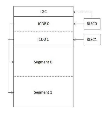
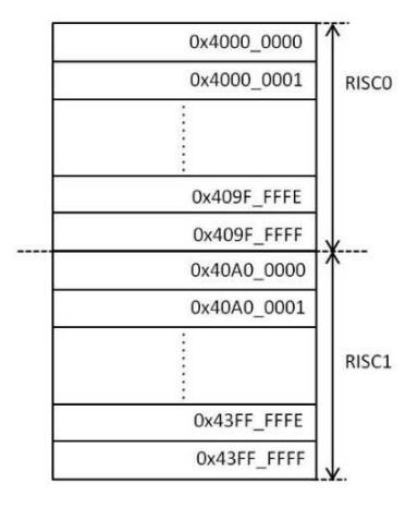
Figure 4 IPC block structure. Figure 5 IPC memory allocation.
4 Processor Resource Allocation
The dual-core processors need to execute concurrent tasks to maximize the benefits. To perform uplink (UL) and downlink (DL) communication between the base station (BS) and a subscriber station (SS) in TDD OFDMA, we incorporated four types of data link tasks, as shown in Table 1. The BS Transmit and BS Receive tasks are performed in the base station, while SS Transmit and SS Receive are performed in the subscriber station. These data link tasks consist of three processing layers, namely the physical layer (PHY), the medium access control layer (MAC), and the network layer. To perform processing division and increase processing parallelism, the data link tasks are divided between RISC1 and RISC0 based on the processing layer. Each processor is allocated as shown in Table 2. RISC0 handles any functions related to processes in the network and MAC layers, while RISC1 handle any functions related to the PHY layer and the RF configuration.
Table 1 Data link tasks. Type Function Communication BS Transmit Transmit data from BS to SS DL BS Receive Receive data from SS to BS UL SS Transmit Transmit data from SS to BS UL SS Receiver Receive data from BS to SS DL
Table 2 Processor functional allocation.
| Processor | Function |
|---|---|
| 1. Physical (PHY) layer | |
| RISC1 | 2. RF configuration |
| 1. Medium access control (MAC) layer | |
| RISC0 | 2. Network layer |
4.1 RISC1 Resource Allocation
RISC1 handles the processing related to the PHY layer. In the proposed system, the physical layer is implemented using a dedicated hardware architecture. In order to communicate with other devices, we make an abstraction layer of this hardware and access it with a specially designated protocol, called Physical Layer Service Application Protocol (PHY-SAP). The main function of PHY-SAP is to establish a connection between the MAC and PHY layers. Since it supports the MAC function, this task is also called lower MAC. It consists of library-calling functions. Besides, RISC1 is also responsible for configuring the RF module during both initialization and run-time.
4.2 RISC0 Resource Allocation
RISC0 performs the rest of the processing for the MAC and network layers. MAC has the function to construct or decode frames and maintain quality of service (QoS). An Ethernet connection is utilized for the network layer. Therefore, RISC0 also handles the Ethernet driver. The dual-core MPSoC performance depends on the parallelism of the data link task processing. The data link task processes based on the previous resource allocation are illustrated in Figures 6-8.
BS Receive task processing is illustrated in Figure 6. There are two types of data decoding in this task: data burst and contention burst. In case of data burst, the data packets are decoded and extracted from burst and the PDU decoder. The information data for the base station are passed to Ethernet. In the case of contention burst, the data are used for controlling the base station (i.e. initial ranging and bandwidth request). It shows that PHY-SAP (Lower MAC) is done in RISC1, while the MAC and network layers are done in RISC0. Both basestation processors work independently and share the burst data in Shared RAM.
SS Transmit task processing is illustrated in Figure 7. Three types of transmitted data are constructed within the MAC layer, namely uplink (UL) burst, initial ranging, and bandwidth request. SS Receive task processing is illustrated in Figure 8. Here, data transfer is similar to the BS Receive task, except it only uses the data burst section. This is because the data receiving mechanism is designed to be as simple as possible and a similar mechanism is the best choice for minimizing the design complexity.
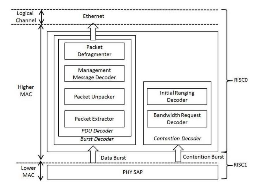
Figure 6 BS Receive task.
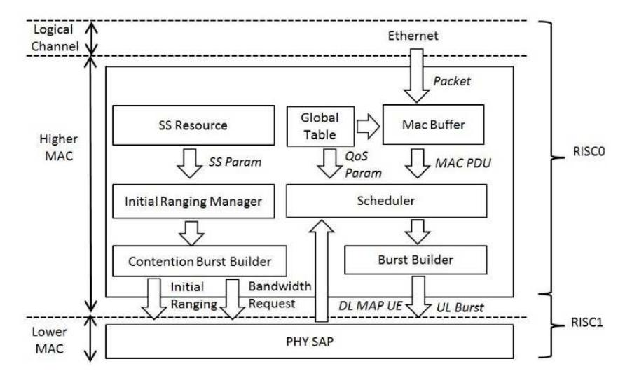
Figure 7 SS Transmit task.
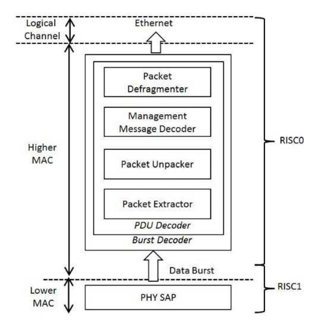
Figure 8 SS Receive task.
5 Network Layer
The network layer has the responsibility to provide the network communication protocol and data exchange. To provide this function, eCos 1.8 is used as the operating system (OS). This layer ensures the communication between the MAC layer and the network layer using Ethernet. All data are packed and then transferred from the MAC layer to an IP packet and vice versa the IP packet is received and then unpacked by the MAC layer for a higher layer.
6 FPGA Implementation
The whole MPSoC including OFDMA PHY was implemented on an FPGA Altera Stratix IV EP4SGX530KH40C3® and set up in a prototyping scale, as shown in Figure 9. The RTL codes were synthesized using Altera Quartus® software. The synthesis area reports can be seen in Figure 10. It was shown that the proposed system only consumed 36% of resources, comprising 117493 combinational ALUTs, 32 memory ALUTs, and 53334 dedicated logic registers. The proposed system was synthesized at 40 MHz clock frequency as the clock frequency for the main system and a clock frequency of 80 MHz was created from the phase locked loop (PLL) for the memory and high-speed bus modules.
Figure 9 The MPSoC prototyping set-up.
| Family | Stratix IV | |
|---|---|---|
| Device | EP4SGX530KH40C3 | |
| Timing Models | Final | |
| Met timing requirements | N/A | |
| 36 % | |
| Combinational ALUTs | 117,493 / 424,960 ( 28 % ) | |
| Memory ALUTs | 32 / 212,480 ( < 1 % ) | |
| Dedicated logic registers | 53,334 / 424,960 ( 13 % ) | |
| Total registers | 53334 | |
| Total pins | 474 / 888 ( 53 % ) | |
| Total virtual pins | 0 | |
| Total block memory bits | 1,429,008 / 21,233,664 ( 7 % ) | |
| DSP block 18-bit elements | 230 / 1,024 ( 22 % ) | |
| Total GXB Receiver Channel PCS | 0/24(0%) | |
| Total GXB Receiver Channel PMA | 0/36(0%) | |
| Total GXB Transmitter Channel PCS | 0/24(0%) | |
| Total GXB Transmitter Channel PMA | 0/36(0%) | |
| Total PLLs | 3/8(38%) | |
| Total DLLs | 0/4(0%) | |
Figure 10 Synthesis reports.
7 System Verification
System verification is required to ensure that the system's functionality is working properly. Here, system verification consisted of a functional simulation, waveform evaluation and application evaluation (i.e. web browsing and video streaming). The Register Transfer Level (RTL) simulator software was used to do the functional simulation and waveform evaluation. The functional simulation verified whether the modules were positioned correctly in the AMBA bus system. A part of this SoC functional simulation can be seen in Figure 11. Here we can see that the OFDMA PHY IP module is mentioned after 'Unknown Device', which is placed as slave 0 ('slv0'). The memory addresses match the designated memory allocations. These ensure that the OFDMA MPSoC is established well.
Figure 11 Established MPSoC architecture.
The bus controller gives output strings that confirm all the module functionalities are working properly. A simple 'hello world' program was also loaded to the SDRAM to check the connection between the SDRAM within the MPSoC. String 'cpu-0 active' is the string from RISC0 and string 'cpu-1 active' is the string from RISC1. These results confirm that the two processors can run the program in parallel. The waveform simulation was needed to check all signaling and related timing in the MPSoC. To ensure the communication between the modules, a testing scenario was designed as described in Table 3. Evaluations were conducted by generating a packet of data and sending it to the destination module. The received data were read and compared to the original data. Identical original and received data means that the sharing mechanism worked properly.
| Scenario | Source | Destination |
|---|---|---|
| RISC1_RISC0 | RISC1 SDRAM | RISC0 SDRAM |
| RISC0_RISC1 | RISC0 SDRAM | RISC1 SDRAM |
| RISC1_eth | RISC1 SDRAM | Ethernet |
| eth_RISC1 | Ethernet | RISC1 SDRAM |
Table 3 Internal communication test scenario.
As an advanced verification scenario, web browsing and video streaming were conducted using two designated MPSoC systems as OFDMA base station (BS) and subscriber station (SS), as depicted in Figure 12. The test environment consisted of two parts, a base station (BS) and a subscriber station (SS). In the BS section, there were PC BS and OFDMA BS (i.e. MPSoC). PC BS was responsible for accessing Internet and determining what kind of data to transmit to the SS section. The data selected by PC BS were processed in OFDMA BS MPSoC and transformed into OFDMA physical signals for wireless transmission to the SS section. In the SS section, the OFDMA signals were received and processed by the OFDMA SS MPSoC to obtain the desired data. When the signals were ready for the user, they were forwarded to PC SS. Several web browsing tests were conducted, one of which is displayed in Figure 13. Meanwhile, video streaming tests were conducted as well, one of which is displayed in Figure 14. We can see that the SS PC can do web browsing and video streaming via the OFDMA communication scheme provided by the proposed MPSoC. This proves that the proposed MPSoC architecture worked as expected.
Figure 12 Advanced verification test scheme.
Figure 13 Web browsing test.
Figure 14 Video streaming test.
8 Conclusion and Future Work
The proposed MPSoC architecture that incorporates an IPC table for OFDMA processing, provides flexible and efficient access to each processor for accessing the shared memory. Therefore, computational resources for data sharing can be maintained as low as possible. The architecture is also scalable to more than two processors with different clock frequencies (heterogeneous MPSoC). The system also supports multi-bus and multi-frequency. The frequency can be set based on the attached module and system requirements. Hence, a low clock frequency can be maintained. The proposed MPSoC system was implemented on an FPGA Altera Stratix IV EP4SGX530KH40C3<sup>®</sup> and only consumed 36% of resources, comprising 11,7493 combinational ALUTs, 32 memory ALUTs, and 53,334 dedicated logic registers. Real-time application tests were conducted for web browsing and video streaming and the results showed that the proposed MPSoC worked properly. The proposed system is a good stepping stone for further investigation of the optimal architecture for OFDMA in terms of performance, speed frequency and power consumption in the future.
Acknowledgements
This article is an extension of a paper presented in the 2015 International SoC Design Conference (ISOCC), Gyeongju-si, South Korea [11]. Furthermore, the authors would like to thank Mr. Kresno Adityowibowo, who has contributed to the Ethernet driver part related to this work.