
1 Introduction
DC-DC converters are widely used in power management technology for the development of modern integrated circuits and systems. The widespread use of portable devices (e.g. digital cameras, cellular phones and tablet computers) require a high-performance DC-DC converter for ensuring the quality of the power supply. In battery-powered systems, a fully charged battery usually possesses a higher voltage than its nominal voltage, while a discharged battery has a lower one. In order to generate a stable power supply voltage a buck-boost converter is generally used because of its wide input voltage range [1-3]. Moreover, a stable voltage is required in high-performance systems to cope with the dynamically varying workload, especially in modern microprocessor systems. When the system switches between idle mode and active mode there is a large
difference in the required current load. Meanwhile, in active mode the processor usually has varying load. Unfortunately, the output current slew rate of the buckboost converter is usually limited by the inductor. Thus, the supply voltage fed by the converter will encounter undershoot or overshoot and deviate from its nominal value. Overshoot may cause a raise in chip temperature, while undershoot may force the processor to insert 'idle' instructions to reduce the load current. Furthermore, the processor may fail to execute any instructions or dismiss some data [4,5]. The aforementioned facts show that the slew rate limitation in the output current must be mitigated and a fast-transient response is an important design consideration in developing a DC-DC converter.
In a buck-boost converter, the incapability of the inductor to suddenly change the current will violate the output voltage range. It will take some time to return the output voltage to its nominal value, resulting in undershoot or overshoot in the output voltage. Furthermore, when the converter works in boost mode it suffers from output current change due to the opposite trends of the output-current change and the output-voltage change.
Several methods and algorithms have been developed to alleviate undershoot and overshoot in the output voltage of buck-boost converters [6-12]. In [6], adaptive pulse skipping and adaptive compensation capacitance techniques were used to reduce the transient response to 59 µs in a 400 mA load. The converter was reported to be able to achieve a fastest transient response of 45 µs under a load current of 200 mA using a hybrid buck-boost feed-forward technique [7]. In general, the transient response can be reduced by using a higher switching frequency. Using a switching frequency higher than 1 MHz may reduce the transient response to under 20 µs [8-12]. In [8], a switching frequency of 3 MHz could support on-duty modulation to achieve a fast line transient response of 17.2 μs at a load change from 10 to 600 mA. Meanwhile, in [11], by utilizing a loaddependent on/off time, the transient response could be improved to 10 µs at a 600 mA load current. Utilization of a higher switching frequency may improve the transient response, but it produces higher switching loss and circuit diagram complexity. The aforementioned studies [8-12] could enhance the quality of the transient response, but undershoot and overshoot in the output voltage were still inevitable. Thus, the development of a new method to support a fast transient response DC-DC converter is of interest.
In this paper, a novel cascaded boost-buck converter architecture is proposed. A similar architecture has been developed for a wireless power transfer system [13] and an electric bus charger [14]. In [13], this architecture was used to perform optimal impedance matching and dynamic load isolation. Meanwhile, the architecture described in [14] was utilized to accommodate the input and battery voltage. However, neither application intended to improve the transient response.
This manuscript is divided into four sections. Section 1 presents the background and an overview of the proposed method. In Section 2, a description of the architecture and the theoretical formulation of the new method as well as the working principle of the proposed converter are discussed. Several relevant simulated cases are presented in Section 3. The experimental results are subsequently analyzed and compared with those obtained in similar experiments on conventional buck-boost converters. Finally, the conclusions are drawn in Section 4.
2 Research Method
Figure 1(a) shows a buck-boost converter that is widely used, while Figure 1(b) shows the proposed boost-buck converter. They both have lower voltage stress on the components due to a non-inverting output voltage [15-17]. The proposed boost-buck converter is a development of the one reported in [18]. It uses separate inductors for the boost stage and the buck stage. An additional shared capacitor \(C_A\) filters the boost-stage output voltage and constitutes the voltage source for the buck stage.
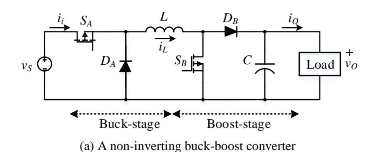
(b) The proposed boost-buck converter
Figure 1 A non-inverting buck-boost converter and the proposed boost-buck converter.
2.1 The Boost-stage
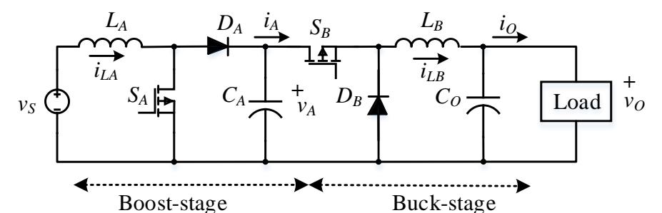
In the proposed boost-buck converter, the boost stage steps up the input voltage, \(v_s\), to the shared capacitor voltage, \(v_A\). Figure 2(a) shows the key waveform when the boost stage operates in discontinuous-current mode (DCM) and continuous-current mode (CCM) with switching period \(T_s\) and duty cycle \(d_A\). When the stage works in DCM, three unique phases appear during each switching period: the charge, transfer, and idle phases [11]. During the charge phase, the power switch \(S_A\) is on, thus the voltage source \(v_s\) energizes the boost-inductor \(L_A\), while the buck stage is energized by the energy stored in the shared capacitor. Meanwhile, in the transfer phase, the power switch \(S_A\) is turned off and the energy stored in the boost-inductor is released and becomes boost-stage output current \(i_A\). When the stored energy in the boost inductor has run out, the stage falls into the idle phase. By applying KVL and KCL the state space representation for the charge phase can be expressed as follows:
\[\begin{bmatrix} \frac{di_{LA}(t)}{dt} \\ \frac{dv_A(t)}{dt} \end{bmatrix} = \begin{bmatrix} 0 & 0 \\ 0 & \frac{1}{C_A R_L} \end{bmatrix} \begin{bmatrix} i_{LA}(t) \\ v_A(t) \end{bmatrix} + \begin{bmatrix} \frac{1}{L_A} \\ 0 \end{bmatrix} v_S\] (1)
Meanwhile, the state space representation for the transfer phase and the idle phase can be formulated as follows:
\[\begin{bmatrix} \frac{di_{LA}(t)}{dt} \\ \frac{dv_A(t)}{dt} \end{bmatrix} = \begin{bmatrix} 0 & -\frac{1}{L_A} \\ \frac{1}{C_A} & -\frac{1}{C_A R_L} \end{bmatrix} \begin{bmatrix}\ni_{LA}(t) \\ v_A(t) \end{bmatrix} + \begin{bmatrix} \frac{1}{L_A} \\ 0 \end{bmatrix} v_S\] (2)
Figure 2 Key wave forms of the boost and buck stages.
When there is no net change in the output current and voltage during a switching period, the stage reaches steady state. From the Eqs. (1) and (2), the output current \(i_A\) in DCM can be expressed as follows:
\[i_A = \frac{v_S^2 d_A^2 T_S}{2(v_A - v_S)L_A} \tag{3}\]
Therefore, boost-stage duty cycle may track boost-stage output current as:
\[d_A = \sqrt{\frac{2i_A(v_A - v_S)L_A}{v_S^2 T_S}} \tag{4}\] when the stage works in CCM, only two unique phases appear: the charge phase and the transfer phase. The changes of output current ∆ and output voltage ∆ within one switching period can be derived as:
\[\Delta i_A = \frac{T_S}{L_A} (v_S - v_A + d_A v_A) \tag{5}\]
\[\Delta v_A = \frac{T_S}{c_A} (i_{LA} (1 - d_A) - i_A) \tag{6}\]
The stage reacts to output current change by determining a new duty cycle in order to change :
\[d_A = \frac{\Delta i_A v_A L_A + (v_A - v_S) v_S T_S}{v_S v_A T_S} \tag{7}\]
The output current condition where the boost stage is at the boundary between DCM and CCM is:
\[i_{O(D/C)} = \frac{(v_A - v_S)v_S^2 T_S}{2v_A^2 L_A} \tag{8}\]
The relationship between the changes of output current ∆ and voltage ∆ can be derived as:
\[\Delta v_A = -\frac{\Delta i_A i_A v_A L_A}{v_S^2 C_A} \tag{9}\]
Eq. (9) clearly states an opposite trend between both parameters. This essential problem implies that the output current increases cause the output voltage to drop and vice versa. This induces an output voltage range violation in the buck-boost converter due to the stage directly supplying energy to the load. Therefore, the stability of the output voltage suffers from an output current change when the buck-boost converter works in boost mode. Although it is possible to alleviate this problem, it will be still inevitable in the transient stage and produce overshoot or undershoot in the output voltage.
2.2 The Buck Stage
The buck stage steps down the shared capacitor voltage, , to the output voltage, . Figure 2(b) shows the key waveform when the buck stage operates in DCM and CCM with switching period and duty cycle . When the stage works in
DCM, three unique phases appear in each switching period: the charge, discharge, and idle phases [11]. During the charge phase, the power switch \(S_B\) is on and thus the voltage source \(v_S\) energizes the inductor \(L_B\). Meanwhile during the discharge phase, the power switch \(S_B\) is turned off and the energy stored in the buck inductor is released to the output capacitor and supplies the load. When there is no more energy stored in the buck inductor, the stage falls into the idle phase. By applying KVL and KCL, the state space representation for the charge phase can be expressed as follows:
\[\begin{bmatrix} \frac{di_{LB}(t)}{dt} \\ \frac{dv_O(t)}{dt} \end{bmatrix} = \begin{bmatrix} 0 & -\frac{1}{L_B} \\ \frac{1}{C_O} & -\frac{1}{C_O R_L} \end{bmatrix} \begin{bmatrix} i_{LB}(t) \\ v_O(t) \end{bmatrix} + \begin{bmatrix} \frac{1}{L_B} \\ 0 \end{bmatrix} v_A\] (10)
Meanwhile, the state space representation for the discharge and idle phases can be formulated as:
\[\begin{bmatrix} \frac{di_{LB}(t)}{dt} \\ \frac{dv_O(t)}{dt} \end{bmatrix} = \begin{bmatrix} 0 & -\frac{1}{L_B} \\ \frac{1}{C_O} & -\frac{1}{C_O R_L} \end{bmatrix} \begin{bmatrix} i_{LB}(t) \\ v_O(t) \end{bmatrix} + \begin{bmatrix} 0 \\ 0 \end{bmatrix} v_A\] (11)
When the stage reaches steady state the output current in DCM can be calculated as:
\[i_O = \frac{v_A - v_O}{2L_B} d_B^2 T_S \left( 1 + \frac{v_A - v_O}{v_O} \right) \tag{12}\]
Therefore, buck-stage duty cycle \(d_B\) may track output current \(i_O\) as follows:
\[d_B = \sqrt{\frac{2i_0 L_B v_0}{v_A (v_A - v_0) T_S}} \tag{13}\]
Meanwhile, when the buck stage works in CCM only two unique phases appear: charge and discharge. By using Eqs. (10) and (11), the changes of buck-inductor current \(\Delta i_{LB}\) and output voltage \(\Delta v_O\) within one switching period \(T_S\) can be derived as Eqs. (14) and (15) respectively:
\[\Delta i_{LB} = \frac{T_S}{L_B} (v_A d_B - v_O) \tag{14}\]
\[\Delta v_O = \frac{T_S}{C_O} (i_{LB} - i_O) \tag{15}\]
In this mode, the stage reacts to output current changes \(\Delta i_O\) by determining a new duty cycle in order to change \(i_{LB}\). From Eq. (14), duty cycle \(d_B\) can be calculated as:
\[d_B = \frac{\Delta i_O L_B + \nu_O T_S}{T_S \nu_A} \tag{16}\]
The output current condition where the buck stage is at the boundary between DCM and CCM is:
\[i_{O(D/C)} = \frac{v_A v_O - v_O^2}{2L_B v_A} T_S \tag{17}\]
2.3 Working Principle of the Boost-Buck Converter
The stability of the output voltage in the buck-boost converter suffers from an output current change when it works in the boost-stage CCM. The upper part of Figure 3(a) shows an example of the waveforms of inductor current \(i_L\) (blue line), diode current \(i_D\) (red) and load current \(i_D\) (black-dashed). As a load current of 1 A is applied at t=1.7 µs, the boost stage reacts by increasing its duty cycle to prolong the charge phase in order to increase the inductor current. However, during this phase no energy is transferred from the inductor to the load. This causes a voltage drop in transient period \(\Delta t + t_{ch}\). The deleterious effect of an output current change is clearly illustrated by the output voltage curve in the lower part of Figure 3(a).
A simplified qualitative way to visualize the different basic operations of the proposed boost-buck converter and a conventional buck-boost converter is to consider the use of the shared capacitor as a temporary energy-storing element. The energy stored in the shared capacitor can be used to maintain the output voltage at the nominal value if its voltage \(v_A\) is higher than the output voltage \(v_O\). Such energy can be defined as \(E_A = \frac{1}{2}C_A(v_A{}^2 - v_O{}^2)\), so that the shared capacitor voltage that must be available when the converter is drawn by a load current of \(i_O\) can be derived as follows:
\[v_A = \sqrt{\frac{2(i_{O(max)} - i_O)v_O v_S^2 T_S + 2(i_{O(max)} - i_O)^2 v_O^2 L_A}{C_A v_S^2} + v_O^2}\] (18)
The actual shared capacitor voltage may not be equal to \(v_A\) as calculated in Eq. (18). In the foregoing analysis, \(v_{A\_ref}\) defines the result of Eq. (18) and \(v_A\) is the actual shared capacitor voltage. To recover the energy balance after an output current change, PID compensation is adopted to return \(v_A\) back to \(v_{Aref}\) by slightly increasing or decreasing the duty cycle for a period of time.
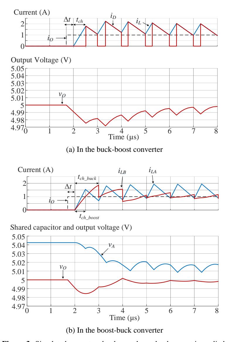
Figure 3 Simulated current and voltage when a load current is applied.
3 Results and Discussions
The proposed boost-buck DC-DC converter is designed to achieve a faster transient response with smaller output-voltage ripple. Several simulations utilizing the system parameters listed in Table 1 were conducted to investigate the performance of the proposed converter. For the sake of verification of the obtained transient response, load current changes were applied to the converter for a short time period.
| Parameters | Symbols | Values | |
|---|---|---|---|
| Input voltage | VS | 3.5 V | |
| Output voltage | Vo | 5 V | |
| Boost-inductance | \(L_A\) | 1 μΗ | |
| Buck-inductance | \(L_{\mathrm{B}}\) | 22 nH | |
| Shared capacitor | \(C_A\) | 33 μF | |
| Output capacitor | Co | 33 µF | |
| Maximum output current | io(max)) | 1 A | |
| Switching frequency | \(f_{\rm c}\) | 1 MH2 | |
Table 1 Parameters of proposed boost-buck converter.
Figure 4 presents a comparison of the simulated transient waveform for current and voltage between a conventional buck-boost converter and the proposed boost-buck converter. In this simulation, an initial step-up load current of 0.2 A was applied at \(t=2.8~\mu s\). Owing to the fact that \(i_0\) was lower than \(i_{O(D/C)}\), the operation mode was set to DCM and a new duty cycle was determined. In the proposed boost-buck converter, the increased duty cycle yields an increase of boost-inductor current \(i_{LA}\) and buck-inductor current \(i_{LB}\). Regarding the output voltage, as stated in Eqs. (4) and (13), the duty cycle of the boost and buck stages of both converters have the same trends as their output voltage, therefore overshoot and undershoot do not occur.
When a load change of 0.6 A was applied at \(t = 9.8 \, \mu s\), \(i_O\) was higher than \(i_{O(D/C)}\). Thus, the converter increased the duty cycle and switched the operation to CCM. In a buck-boost converter, an increase of the boost-stage duty cycle introduces an output voltage drop. In the proposed converter, however, an increase of the boost-stage duty cycle results in a decrease of shared capacitor voltage \(v_A\) only. In spite of this, as long as \(v_A\) is greater than \(v_O\), the output voltage can be properly kept constant by the buck stage. By comparing the output current injected into the output capacitor it can be seen that the diode current, \(i_D\), in the buck-boost converter is discontinuous or pulsating, while the buck-inductor current, \(i_{LB}\), in the proposed converter is a sawtooth. These phenomena ensure that the output-voltage ripple of the proposed converter is lower than that of a conventional buck-boost converter.
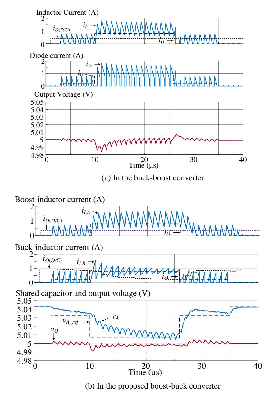
Figure 4 Simulated waveforms for current, voltage and duty cycle.
As stated in Eq. (16), the duty cycle of the boost-stage CCM depends on outputcurrent change ∆ and the DC level of the input voltage and output voltage . When a conventional buck-boost converter is in the boost stage, the converter
reacts to a change in the duty cycle according to \(\Delta i_O\) only because of the fixed values of \(v_S\) and \(v_O\). Therefore, in the case of a light to heavy load change, the duty cycle is raised for certain switching periods and returned back to the steady-state value afterwards. Meanwhile, in the proposed converter, the boost-stage determines the duty cycle according to \(\Delta i_O\) and shared-capacitor voltage \(v_A\). Due to the opposite reaction between both parameters, the variation of boost-stage duty cycle \(d_A\) in the proposed converter is smaller than in a conventional converter. The same trend also occurs to boost-inductor current \(i_{LA}\). This makes the boost stage of the proposed converter seem to have a more sluggish response than that of a conventional one.
As the load becomes lower, the converter determines a lower duty cycle to decrease the inductor current. In a buck-boost converter, a lower boost-stage duty cycle results in a decrease of the charge phase while increasing the transfer phase. More time for the transfer phase increases \(i_D\) and causes an upward violation of the output voltage range. Meanwhile, in the proposed converter more time for the transfer phase increases boost-stage output current \(i_A\) and shared capacitor voltage \(v_A\). However, a decrease in output load current \(i_O\) will be followed by an increase in \(v_{A\_ref}\), as shown by Eq. (18). Consequently, \(v_A\) will be able to reach \(v_{A\_ref}\) faster.
In the proposed converter, when the output current changes, the buck-stage determines the corresponding adjustment amount of the duty cycle according to Eqs. (13) or (16) to change the buck-inductor current in order to keep the output voltage constant at its nominal value. Due to the inductor's tendency to resist changes in current, the output current slew rate is fundamentally limited due to the presence of the buck inductor. To allow more rapid changes in the buck-inductor current, the level of inductance may be reduced. This can be done because the proposed architecture uses separate inductors for the boost and buck stages. In contrast with a conventional buck-boost converter, which uses the same inductor for both stages, reducing the inductance may improve the transient response, but it will increase the output-voltage ripple when it is in the boost stage.
The level of buck inductance must be carefully determined. Using a smaller buck inductance will reduce \(i_{O(D/C)}\) and thus may force the buck stage to work in DCM for more cases and increase the output-voltage ripple. The proposed converter uses a buck inductance of 22 nH. By harnessing the energy stored in the shared capacitor, the buck stage allows the current to flow through the buck inductor with a rate of change up to 1.91 A/\(\mu\)s when the maximum load current is applied after no-load condition. Therefore, this stage is able to recover the output voltage to 2 \(\mu\)s. By comparing the transient response time and output-voltage ripple
between a conventional buck-boost converter and the proposed converter in Figure 3 and Figure 4 it is clear that the transient response time of the proposed converter is shorter than that of a conventional one. Moreover, to further enhance the transient response and efficiency, several methods have been introduced to further develop the proposed converter [19]-[22].
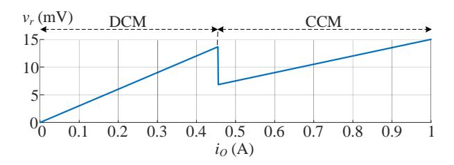
Figure 5 The output-voltage ripple as the output current.
The proposed converter may provide a better output-voltage ripple when drawn by a large output current and the buck stage works in CCM. In this case, buck-stage duty cycle approaches one, thus , , and constitute a second-order filter. Hence, the output-voltage ripple can be effectively diminished. Figure 5 shows the output-voltage ripple as the output current. The maximum value of the output-voltage ripple is 13.6 mV when the buck stage works in DCM and 15 mV when it works in CCM.
Table 2 summarizes the measured characteristics of the published DC-DC converter. Using a switching frequency of 1 MHz, the pseudo-current dynamic acceleration from [12] can be utilized to improve the transient response to 2 µs. However, the proposed boost-buck converter provides a better output voltage quality due to its lower output-voltage ripple. Therefore, the performance of the proposed converter is comparable with that of a fast-transient DC-DC converter. The comparison clearly shows the improvements of the proposed boost-buck design, which provides one of the fastest transient responses with lower outputvoltage ripple.
This research may challenge future researchers in the DC-DC converter field. As shown in Figure 1, the proposed converter uses two switches that work simultaneously. Compared to a conventional converter, this converter may have efficiency issues due to the double switching process. Future research is expected to address the possibility of degradation of the conversion efficiency. In this case, the method of zero-voltage zero-current switching can be developed to improve the conversion efficiency [23,24]. Thus, the proposed boost-buck converter is suitable for practical applications, presenting an extremely fast transient response and low output-voltage ripple.
Table 2 Performance comparison of recent techniques developed in DC-DC converter.
| Technique | \(v_S\) and \(v_O\) | \(i_{0(max)}\) | \(f_S\) | \(v_{r(max)}\) | \(t_{r(min)}\) | L/C |
|---|---|---|---|---|---|---|
| Adaptive pulse skipping and | 2.7~4.5 V | 900 | 1 | N/A | 59 μs | 2.2 μΗ/20 μF |
| compensation capacitance [6] | 3 V | mA | MHz | 17/11 | @400 mA | |
| Hybrid buck-boost feedforward [7] | 2.7~4.5 V | 500 | 700 | > 200 mV | 45 μs @200 mA | 4.7 μΗ/47 μF |
| 3.3 V | mA | kHz | ||||
| Direct path skipping and on-duty modulation [8] | 3.0 V 2.8~5.5 V | 1 A | 3 MHz | 88.3 mV | 17.2 μs @600 mA | 2.2 μΗ/33 μF |
| Hysteretic-current- mode [9] | 2.5~5 V | 400 | ≤1.66 | 15 mV | 15 μs | 1 μH/10 μF |
| 3.3 V | mA | MHz | @290 mA | |||
| Power-tracking with fast dynamic voltage | 2.5~4.5 V | 400 | 5 | > 175 mV | 15 μs | 1 μH/0.88 μF |
| scaling [10] | 2~4 V | mA | MHz | > 173 III V | @300 mA | ι μιν σισσ μι |
| Load-dependent on/off time [11] | 3.3 V 1.8~5.0V | 800 mA | 3.3 MHz | 90 mV | 10 μs @600 mA | 1.5 μH/10 μF |
| Pseudo-current | 3.3 V | 200 | 1 | 2 μs | ||
| dynamic acceleration [12] | 1V~4.5V | mA | MHz | 80 mV | @200 mA | 22 μH/10 μF |
| Boost-buck architecture | 3.5~6 V | 1 | 15 37 | 2 μs | \[1{+}0.022~\mu\text{H}/\] | |
| (simulated in this work) | 5 V | 1 A | MHz | 15 mV | @1 A | 33+33 μF |
\(v_S/v_O = \text{input/output voltage}\)
\(i_{O(max)}\) = maximum load current
\(f_S\) = switching frequency
\(v_{r(max)}\)= maximum output-voltage ripple
\(t_{r(min)}\) = minimum transient response time
L/C = capacitance and inductance used
4 Conclusion
A novel cascaded boost-buck converter architecture was proposed to improve the transient response of the DC-DC converter. The converter consists of a cascaded configuration of the boost and buck stages. The boost stage provides sufficient energy in a shared capacitor to supply the buck stage by converting the input voltage to the shared capacitor voltage. Meanwhile, the buck stage converts the shared capacitor voltage to the output voltage. By defining the shared capacitor voltage higher than the output voltage, the buck stage unitizes the energy stored in the shared capacitor to keep the output voltage at its nominal value. The proposed converter uses separate inductors for the boost and buck stages. By using a low buck inductance, the buck stage allows rapid changes in the output current. The simulation results showed that the recovery time can be improved to 2 μs with a step-up load current change of 1 A with a maximum output-voltage ripple of 15 mV. The proposed boost-buck converter achieves a fast transient response with low output-voltage ripple and rapidly generates a stable output voltage despite load current variation.
Acknowledgements
The research is supported by Sekolah Tinggi Teknologi Adisutjipto under strategic research grant No. 026/K2.1/P3M/V/2019.