
1 Introduction
Metamaterials and metasurfaces are engineered, or man-made materials, which have received a great deal of attention in recent years [1-3]. Most arranged metamaterials and metasurfaces use split ring resonators (SRR) or complementary split ring resonators (CSRR) to produce negative effective permeability in a limited frequency range [4, 5]. The addition of a thin wire or a stripline is commonly able to achieve a negative permittivity [6]. The integration of an SRR with a thin wire or a stripline is expected to produce a double negative index to comply with the requirements of metamaterials and metasurfaces. Moreover, a periodic pattern on the microstrip patch is also able to produce a high
impedance surface (HIS) to absorb electromagnetic (EM) waves [7, 8]. The design of artificial surfaces to absorb EM waves has been considered with numerous applications [9-11].
Principles of destructive and phase cancellation have been proposed using metasurface absorbers with an L-shaped design for energy harvesting [9]. It evolved from a chiral metasurface with circular polarization conversion. Energy harvesting using a metasurface absorber has also been developed, with a 4 × 4 metamaterial structure with absorptivity higher than 99% at a frequency range of 6.70 GHz to 8.25 GHz [10]. Moreover, an axisymetric metasurface absorber has been designed to reduce the specific absorption rate (SAR) for 5G communication [11]. The performance was analyzed using the SAR Head Hand and Phone model and it was able to cut down the SAR of the antenna by more than 75%. The principle of a metasurface absorber is similar to a guard trace for suppressing electromagnetic coupling between elements [12].
A microstip structure consists of a patch and a groundplane made of a conductor that clamps a dielectric material [13]. The structure can be modeled as a transmission line model, where all impedance components of the microstrip are parallel to each other and since the ground plane is fully covered by the conductor, it can act as a shorted component. An EM wave absorber can be modeled and synthesized as a transmission line since its structure is that of a microstrip and the thickness of the dielectric material as one of its primary parameters is known, so the impedance of its patch can be synthesized with a theoretical approach [14,15]. The theoretical approach synthesizes the impedance of the patch pattern as confirmation of a surface with high impedance.
Designing an EM wave absorber can start with using a single unit cell with adequate settings to create an unlimited pattern to simplify the computation [16]. It is set towards linear excitation and performs absorption related to a single linear excitation. Moreover, a finite pattern can be simulated with the relevant conditions for measurement, with then configuration the same as the simulation settings [17]. Experimentation with the EM wave absorber is one of the major steps in the development of an EM wave absorber as part of the validation process. Free space measurement methods with one port typically verify the EM wave absorber's performance with scattering parameters, while two ports were incorporated to examine EM wave absorber polarization [18]. These measurements are performed using Vector Network Analyzer (VNA) to compare a signal generator as the transmitter and a spectrum analyzer as the receiver.
In this paper, the design of an EM wave absorber formed by SRR with a stripline is presented. Along with the design using single unit cells, a theoretical approach is proposed to synthesize the impedance of a patch structure made of SRR with a stripline. As validation of the design, a single unit cell was simulated into a finite array with excitation of the plane wave and the boundary conditions of radiation.
Consequently, the measurement configuration used two horn antennas that were connected to a signal generator as the transmitter and a spectrum analyzer as the receiver. The experimental characterization of the EM wave absorber was normalized with perfect reflection with the same measurement distances of 250 mm, 500 mm, 750 mm, and 1,000 mm and the angles of excitation between stripline and horn antennas at \(0^{\circ}\), \(45^{\circ}\), and \(90^{\circ}\).
2 Principle of EM Wave Absorber
The principle of an electromagnetic wave absorber for reflection and transmission plane waves is shown in Figure 1(a) [19]. The incident plane wave \(E_0^+\) appears through a vacuum, which is supposed to have zero conductivity to a resistive material presumed with non-zero conductivity. The resistive material can be several materials, depending on the resultant of its constitutive material parameters. Since the impedance of a vacuum is unequal to the impedance of a resistive material, there is a mismatch impedance yielding a reflected wave, \(E_0^-\), with the value given by Eq. (1):
\[E_0^- = \Gamma_0 E_0^+ \tag{1}\]
Meanwhile, for a transmitted plane wave, the incident plane wave \(E_{ms}^+\) can be expressed as follows:
\[E_{ms}^{+} = T_0 E_0^{+} \tag{2}\] and the constitutive parameters of the resistive material are the conductivity of \(\sigma_{ms}\), the permeability of \(\mu_{ms}\), and the permeability of \(\varepsilon_{ms}\).
Following the resistive material, there are a dielectric material and a perfect conductor at the end of the EM wave absorber. The impedance of the resistive material is not equal to the impedance of the dielectric material, so there is a reflected plane wave that can be calculated using Eq. (3):
\[E_{ms}^- = \Gamma_{ms} E_{ms}^+, \tag{3}\] while the incident wave through the dielectric medium can be evaluated with Eq. (4):
\[E_d^+ = T_{ms}E_{ms}^+. (4)\]
2.1 Circuit Model
The constitutive parameters of the dielectric material are the conductivity of \(\sigma_d\), the permeability of \(\mu_d\), and the permittivity of \(\varepsilon_d\). Hence, the impedance of the resistive material and the dielectric material, \(\eta_{ms}\) and \(\eta_d\), can be defined with Eqs. (5) and (6), while the propagation constant of both materials, \(\gamma_{ms}\) and \(\gamma_d\), can be calculated using Eqs. (7) and (8):
\[\eta_{ms} = \sqrt{\frac{j\omega\mu_{ms}}{\sigma_{ms} + j\omega\varepsilon_{ms}}},\tag{5}\]
\[\eta_d = \sqrt{\frac{j\omega\mu_d}{\sigma_d + j\omega\varepsilon_d}},\tag{6}\]
\[\gamma_{ms} = \sqrt{(j\omega\mu_{ms})(\sigma_{ms} + j\omega\sigma_{ms})},\tag{7}\]
\[\gamma_d = \sqrt{(j\omega\mu_d)(\sigma_d + j\omega\sigma_d)}.\] (8)
The perfect conductor has infinite conductivity and using Eq. (5), where \(\sigma_c \approx \infty\), the impedance of the conductor will be equal to zero. The reflection coefficient at the border, \(\Gamma_d\), will equal to -1, which means that all the incident waves from the dielectric material will be reflected back and the transmitted wave in the perfect conductor, \(E_c^+\), will be zero.
Figure 1 Metasurface EM absorber using an SRR and a stripline, (a) EM absorber model, (b) circuit model, (c) T-Network for dielectric.
The circuit model for an EM wave absorber is designed based on the principle of the EM wave absorber, which is illustrated in Figure 1(b) [14]. It consists of a resistive substrate with several components, a dielectric substrate, and a perfect conductor as ground plane. The impedance of the resistive substrate, \(Z_{ms}\), the impedance of the dielectric, \(Z_d\), and the impedance of the groundplane, \(Z_g\), are represented by a parallel structure. The resistive substrate is depicted as parallel admittance, \(\frac{1}{Z_{ms}}\), which is equal to \(\frac{1}{R_{ms}+jX_{ms}}\), since the total impedance of the resistive substrate is in the form of real and imaginary parts of the impedance. The ground plane is represented by a short circuit, while the dielectric substrate, \(Z_d\), constitutes to the impedance of T-network matrix equation (9), as illustrated in Figure 1(c) [14,20]:
\[[Z_d] = \begin{bmatrix} Z_{d_{11}} & Z_{d_{12}} \\ Z_{d_{21}} & Z_{d_{22}} \end{bmatrix}, \tag{9}\] where = 12 and = 11 − 12.
The value of the matrix components can be calculated using Eqs. (10) and (11):
\[Z_{d_{11}} = Z_{d_{22}} = Z_d \coth(\gamma_d d),\] (10)
\[Z_{d_{12}} = Z_{d_{21}} = \frac{Z_d}{\sinh(\gamma_d d)'} \tag{11}\] where is the propagation constant and is the thickness of the dielectric substrate. The characteristics of dielectric subtrates that are implemented to configure a EM wave absorber impact the impedance and propagation constant of the dielectric substrates.
The total impedance of the circuit model for a multilayer EM wave absorbers, , can be achieved by calculating all parallel components as given in Eq. (12):
\[Z_T = \frac{\left(\frac{Z_S Z_p}{Z_S + Z_p} + Z_p\right)\left(\frac{1}{Z_{mS}}\right)}{\left(\frac{Z_S Z_p}{Z_S + Z_p} + Z_p\right) + \left(\frac{1}{Z_{mS}}\right)} \tag{12}\] and the reflection coefficient at the border of the EM wave absorber and the vacuum can be calculated using Eq. (13):
\[\Gamma_t = \frac{Z_T - Z_0}{Z_T + Z_0'},\tag{13}\] where is the total impedance of the EM wave absorber with the circuit model, which consists of resistive substrate, dielectric substrate, and groundplane.
The absorption, which corresponds to the reflection coefficient and the transmission coefficient, can be described with Eq. (14):
\[A = 1 - |\Gamma^2| - |T^2|, \tag{14}\]
since it is a fully grounded EM wave absorber, the transmission coefficient will be equal to zero and the absorption can be calculated using Eq. (15):
\[A = 1 - |\Gamma^2|. \tag{15}\]
2.2 Frequency Responses of X-Band Metasurface EM Wave Absorber
The absorption of a metasurface EM wave absorber is characterized by the alteration of the real and the imaginary part of impedance with respect to Eq. (15), as shown in Figure 2. The solid line representsthe changes of the absorption level, after the conversion of the real part of . The impedance of is 0.0041 + j0.0655 Ω, 0.0028 + j0.0655 Ω, and 0.0016 + j0.0655 Ω, has an absorption level of 0.97, 0.92, and 0.84, respectively, at a frequency of 10 GHz. Along with the decrease of the real part of the impedance, the absorption level is declining.
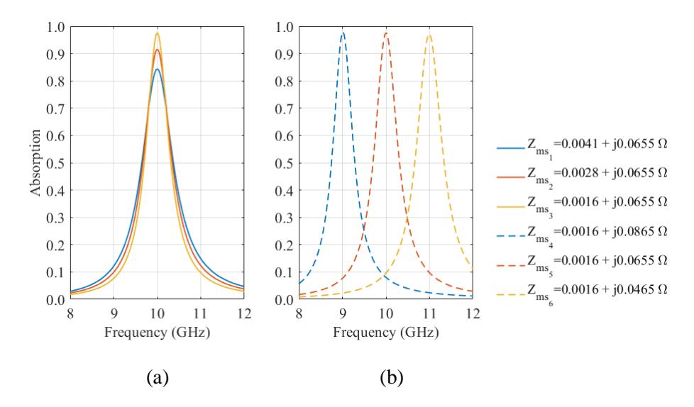
Figure 2 Frequency responses of the real and the imaginary part of the impedance.
The dotted line illustrates the variance of the imaginary part of the impedance, which the impedance of is 0.0016 + j0.0865 Ω, 0.0016 + j0.0655 Ω and 0.0016 + j0.0465 Ω, the frequency responses are 8.98 GHz, 10.02 GHz, and 11 GHz, respectively, with the same level of absorption, i.e., 0.97. This characterization shows that the imaginary part of the impedance shifts the frequency responses, and the real part of the impedance alters the absorption level.
3 Design and Simulation
3.1 Single Unit Cell of X-Band Metasurface EM Wave Absorber
The proposed circuit model of the EM wave absorber was compared with the design of an EM wave absorber formed by an SRR and a stripline, which works at the X-band. The SRR-based X-band wave absorber with stripline was designed on an FR4 epoxy dielectric substrate with a groundplane width of and a separation among unit cell of . The SRR has a width of and an SRR gap of , while the width of the stripline is . The thickness of the dielectric substrate is and the space between SRR and stripline is . The dimensions of each EM wave absorber formed by SRR with stripline in a single unit cell are tabulated in Table 1.
| Parameter | Description | dimension (mm) |
|---|---|---|
| 𝑊𝑔 | Unit cell size | 3.48 |
| 𝑠𝑠𝑟 | SRR separation | 0.26 |
| 𝑊𝑠𝑟 | SRR width | 0.26 |
| 𝑔𝑠𝑟 | SRR gap | 0.30 |
| 𝑤𝑠𝑙 | Stripline width | 0.36 |
| 𝑡𝑑𝑠 | Dielectric substrate thickness | 1.60 |
| 𝑠𝑑𝑠 | Separation of dielectric substrate | 0.20 |
Tabel 1 Dimensions of parameters for each unit cell.
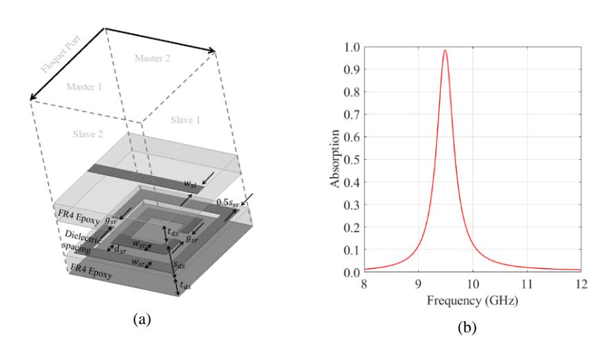
Figure 3 EM wave absorber simulation: (a) design of the single unit cell, (b) result.
As the circuit model in Figure 1(b) shows, the resistive substrate consists of an SRR made of copper, a space made of vacuum, a dielectric substrate made of FR4 epoxy, and a stripline made of copper. The design of the X-band wave absorber formed by SRR with stripline is described in Figure 3(a) and it was simulated with 3D electromagnetic simulation software. In the simulation, the boundary condition was set to produce an unlimited array of split ring resonators with a stripline. The Master and Slave boundary condition was used with the excitation of a Floquet port. This setting was used to perform an unlimited array while the design only uses a single unit cell. The simulation result showed a maximum absorption of 0.98 at a frequency of 9.48 GHz with bandwidth of absorption in the range of 9.44 GHz to 9.56 GHz, which was limited to 0.90 absorption, as depicted in Figure 3(b).
3.2 Syntesizing X-Band Wave Absorber Impedance with Theoretical Approach
Figure 4 shows the performance of the X-band EM wave absorber formed by SRR with a stripline, reflecting a variation of separation among the unit cells, . The variation of this parameter was set from 0.30 mm to 0.70 mm, which produces variation of the impedance of the resistive substrate. The unit cell separation at 0.30 mm, 0.40 mm, 0.50 mm, 0.60 mm, and 0.70 mm can achieve maximum absorption of 0.99, 0.97, 0.96, 0.95, and 0.94, at a frequency center of 9.40 GHz, 9.78 GHz, 10.12 GHz, 10.42 GHz, and 10.74 GHz, respectively.
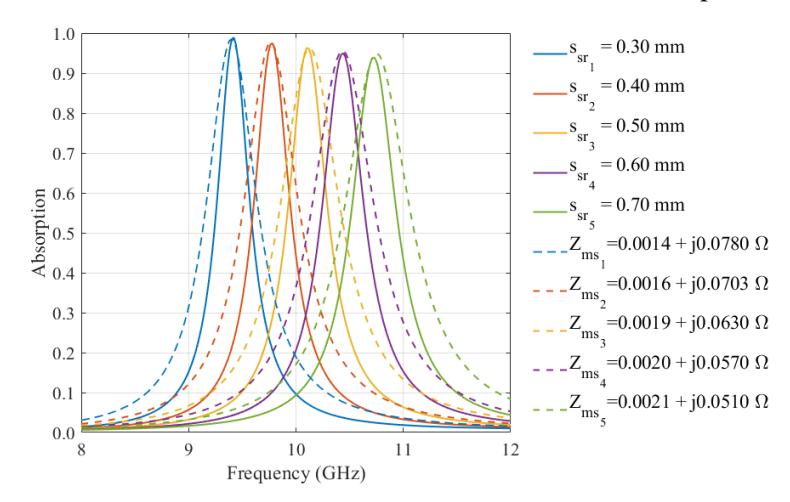
Figure 4 Impedance syntesis using a theoritical approach.
These simulation results were approached with the theoretical approach as described by Eq. (12) and (15), with a corresponding response as with impedance values of 0.0014 + j0.0780 Ω, 0.0016 + j0.0703 Ω, 0.0019 + j0.0630 Ω, 0.0020 + j0.0570 Ω, and 0.0021 + j0.0510 Ω, with a maximum absorption of 0.98, 0.97, 0.95, 0.96, and 0.95, at a frequency center of 9.38 GH, 9.74 GHz, 10.16 GHz, 10.44 GHz, and 10.76 GHz, respectively.
Furthermore, the simulation bandwidth of 0.12 GHz constantly not change as the alteration of separation of the unit cells, however, the theoritical bandwidths of 0.16 GHz, 0.18 GHz, 0.18 GHz, 0.18 GHz, and 0.18 GHz, corresponded with impedance values of 0.0014 + j0.0780 Ω, 0.0016 + j0.0703 Ω, 0.0019 + j0.0630 Ω, 0.0020 + j0.0570 Ω, and 0.0021 + j0.0510 Ω, respectively. Separation of unit cells at 0.30 mm, 0.40 mm, 0.50 mm, 0.60 mm, and 0.70 mm was equal to an impedance of 0.0014 + j0.0780 Ω, 0.0016 + j0.0703 Ω, 0.0019 + j0.0630 Ω, 0.0020 + j0.0570 Ω and 0.0021 + j0.0510 Ω, respectively, which is in accordance with the simulation and the theoretical results.
3.3 Array Unit Cell of X-Band Metasurface EM Wave Absorber
The design of a single unit cell uses the respective boundary conditions to perform an unlimited array of SRR with stripline with simple compution to achieve optimal EM wave absorber performance. Moreover, the design of the single unit cell should be verified with a simulation using a finite array of unit cells. This method has the objective of performing a simulation process that has similar configurations with later experiments set up, which may be a verification process by performing a finite array of SRRs with striplines.
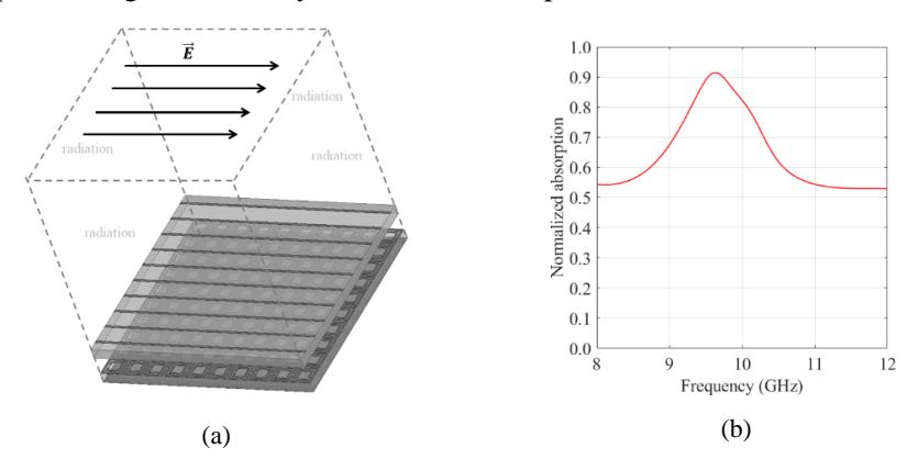
Figure 5 EM wave absorber simulation: (a) finite array with radiation boundary conditions, (b) result.
For designing an array of EM wave absorbers, the boundary conditions are set to radiation with linear excitation parallel to the stripline. The array of EM wave absorbers consisted of a 10 × 10 SRRs with striplines as shown in Figure 5(a) and the result of the simulation is shown in Figure 5(b). The maximum absorption for 10 × 10 SRR with stripline with linear excitation was 0.91 at a frequency of 9.6 GHz. The minimum absorption was 0.54 and 0.53 at a frequency of 8 GHz and 12 GHz, respectively. Moreover, the bandwidth of absorption was 0.25 GHz, which is limited to a value of absorption higher than 0.9, or in the range of 9.50 GHz to 9.75 GHz.
4 Implementation and Measurement
4.1 Free Space Measurement for EM Wave Absorber Using Two Horn Antennas
Two identical horn antennas were connected to a signal generator as the transmitter and the other was connected to a spectrum analyzer as the receiver. The signal generator transmitted \(P_{T_x}\) as power is transmitted throught a coaxial cable with a cable loss of \(L_{coax}\), and propagated to the medium with the amplification of horn antenna gain \(G_H\). The signal was radiated in the medium with a propagation loss of \(L_{path}\) and received by the device under test (DUT) at power of absorption, \(P_{dut}\).
Figure 6 Free space measurements model using two horn antennas.
Furthermore, the transmitted signal will be absorbed by the DUT and part of the signal will be reflected back through the medium with a propagation loss of \(L_{path}\) by the receiver horn antenna with a gain of \(G_H\), and transmitted to the spectrum analyzer at a received power of \(P_{R_x}\) through a coaxial cabel with a cable loss of \(L_{coax}\). A model of free space measurement using two horn antennas is shown in Figure 6. The received power, \(P_{R_x}\), can be calculated using Eq. (16):
\[P_{R_{\chi}}(dBm) = P_{T_{\chi}} - 2L_{coax} + 2G_{H} - L_{path} - P_{dut},\] (16)
and the absorption power of the DUT, \(P_{dut}\), is equivalent to Eq. (17):
\[P_{dut}(dB) = P_{T_x} - 2L_{coax} + 2G_H - L_{path} - P_{R_x}.\] (17)
4.2 Experimental Configuration
The realization of the X-band EM wave absorber formed by SRR with stripline was structurally printed on an FR4 epoxy dielectric substrate with a finite array of 80-unit cells × 80-unit cells, equal to 278.4 mm × 278.4 mm. The bottom layer of the X-band wave absorber was made of a printed fully conducting material, while the SRR was printed on top of the first layer of the FR4 epoxy dielectric substrate, and the stripline was printed on top of the second layer of the FR4 Epoxy dielectric substrate, as depicted in Figure 7.
Figure 7 Realization of the X-band wave absorber using SRR with stripline.
The performance of the X-band EM wave absorber measured by SRR with stripline was achieved by using two horn antennas. The first horn antenna was connected to a signal generator as the transmitter and the second horn antenna was connected to a spectrum analyzer as the receiver, as shown in Figure 8, corresponding with the measurement model in Figure 6. The X-band EM wave absorber formed by SRR with stripline was treated as the DUT and was tested with four measurement distances, 250 mm, 500 mm, 750 mm, and 1,000 mm. This had the purpose of measuring in the near field and far field and also to validate the normalized absorption as proposed measurement methods. Moreover, the measurement distance at various values was expected to validate the simulation process with plane wave excitation. Moreover, the measurement also involved two ideal conditions of absorption and reflection. The full absorption used a fully absorbent material (Figure 8(a)) and the perfect reflection used a metal plate with the same dimensions as the EM wave absorber, i.e., 278.4 mm × 278.4 mm (Figure 8(b)). The full absorption condition and perfect reflection were considered as performance comparison for the SRR with stripline, while the perfect reflection was measured with the same distances, antenna orientation, and size, which can be used as normalization factor to achieve the real performance of the X-band EM wave absorber formed by an SRR with a stripline.
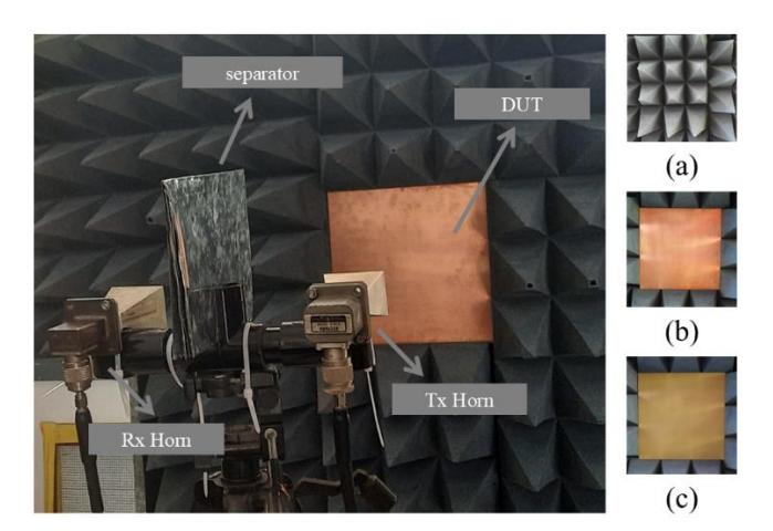
Figure 8 Measurement configuration: (a) fully absorbent material, (b) 278.4 mm × 278.4 mm of metal plate, (c) 278.4 mm × 278.4 mm of SRR with stripline.
4.3 Characterization Result
The absorption of DUT is analyzed in this section. The absorption was performed in terms of normalized absorption to compensate for the propagation loss, the cable loss, and the antenna gain. Normalization was performed using the measurement result for a metal plate with a size of 278.4 mm × 278.4 mm with the same measurement distances. Moreover, the performance of a fully absorbent material was measured as a comparison. The metal plate and the fully absorbent material measurement are shown in Figures 9 to 11, since it is assumed that the surface area has a constant ratio along the changes of measurement distance.
Figure 9 shows the values of free space at a distance of 250 mm, 500 mm, 750 mm, and 1,000 mm, with the orientation of horn antennas at 0°, which is related to the orientation of the stripline, i.e., the transmitter and receiver horn antennas are parallel with the orientation of the stripline. At a distance of 250 mm, the normalized absorption of the metal plate fluctuated from absorption of 0.50 to 0.76, however, the normalized absorption of SRR with stripline fluctuated from 0.40 to 0.99 and the normalized absorption of the cone as a fully absorbent material was stable at 1. The DUT can be categorized as an absorber when the absorption is higher than 0.90, with the results for the SRR and stripline could be a good absorber at a frequency of 8.63 GHz to 9.15 GHz or a bandwitdh of SRR with stripline of 0.52 GHz at a measurement distance of 250 mm.
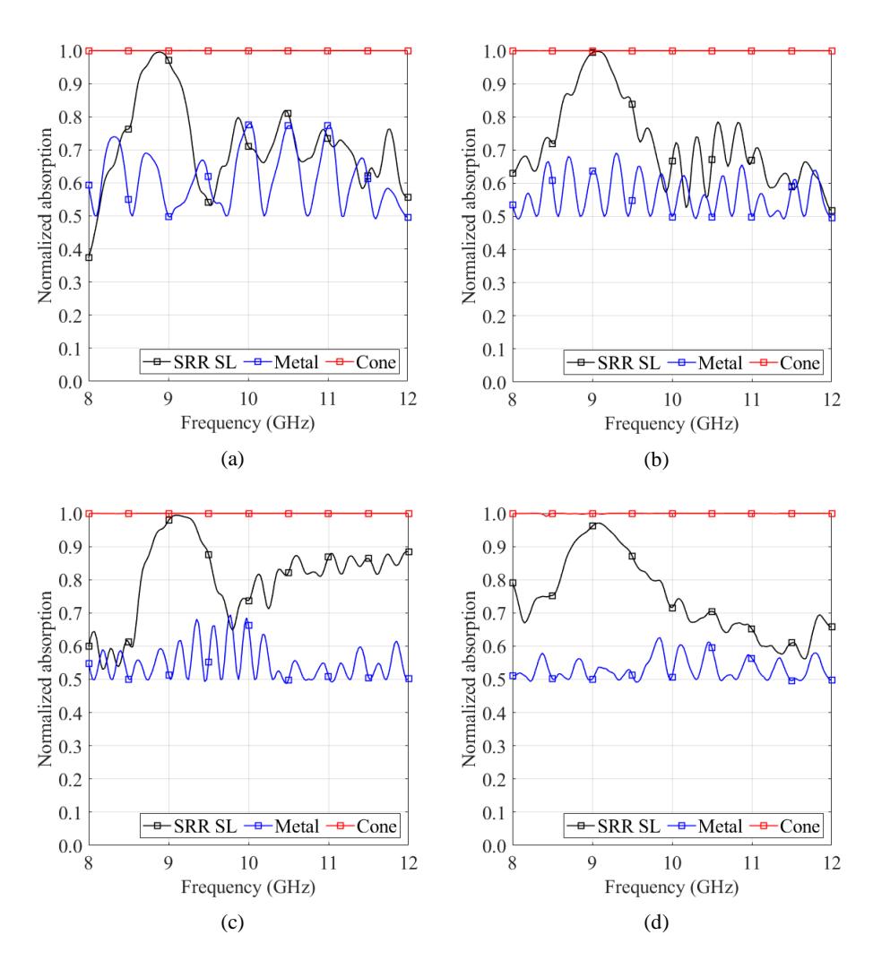
Figure 9 Measurement of open space characterization using designated scenarios and distances at an antenna orientation of °: (a) 250 mm, (b) 500 mm, (c) 750 mm, (d) 1,000 mm.
The maximum normalized absorption was 0.98, 0.99, 0.99, and 0.99, at a frequency center of 8.98 GHz, 8.85 GHz, 9.20 GHz, and 9.25 GHz, for an antenna orientation of 45° with a measurement distance of 250 mm, 500 mm, 750 mm, and 1,000 mm, respectively, as described in Figure 10.
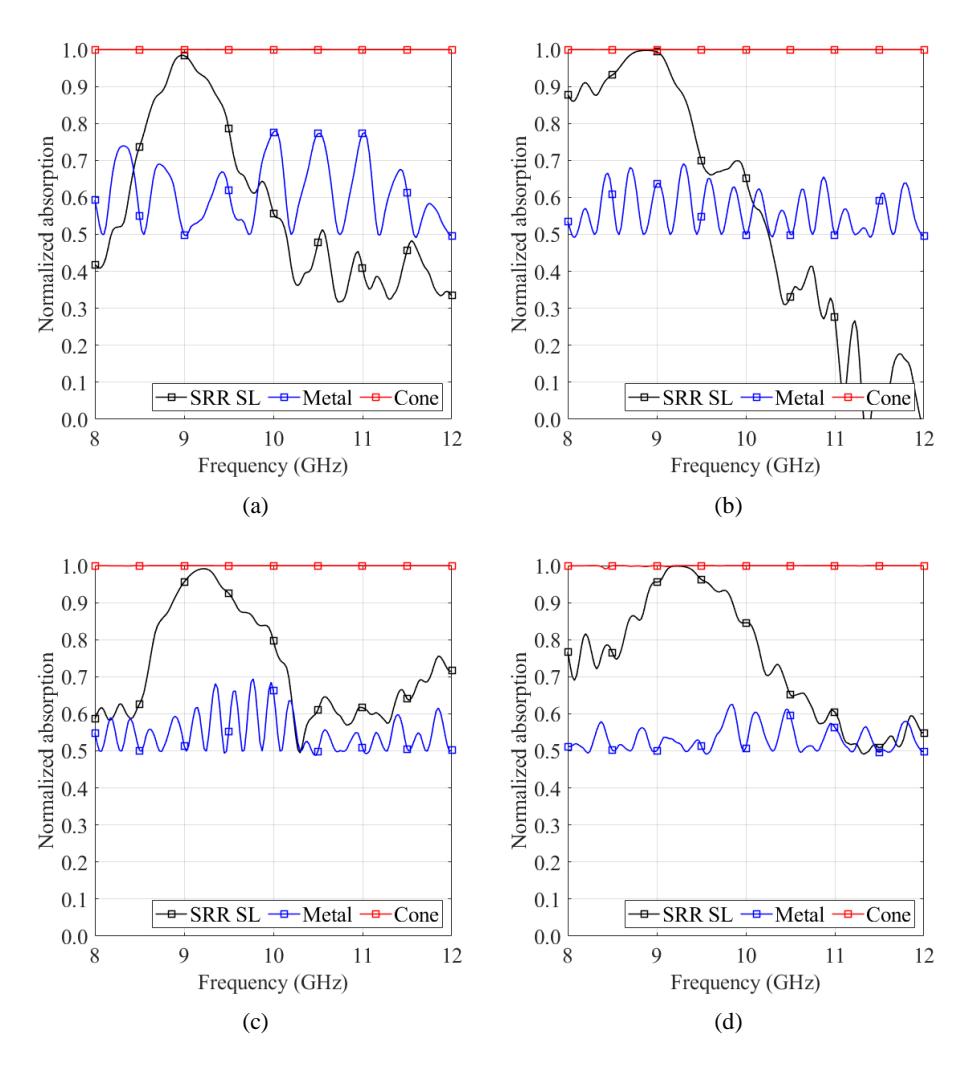
Figure 10 Measurement of open space characterization using designated scenarios and distances at an antenna orientation of °: (a) 250 mm, (b) 500 mm, (c) 750 mm, (d) 1,000 mm.
The bandwidth of normalized absorption was 0.52 GHz for a measurement distance of 250 mm and it increased to 63.46%, 34.62%, and 86.54%, for measurement distances of 500 mm, 750 mm, and 1,000 mm, respectively. Figure 11 plots the performance of normalized absorption at a distance of 250 mm, 500 mm, 750 mm, and 1,000 mm, with an antenna orientation of 90°, or the transmitter and receiver horn antennas were perpendicular to the stripline of Xband wave absorber. In this condition, the bandwidth of normalized absorption was 0.77 GHz, 2.05 GHz, 1.90 GHz, and 1.52 GHz, for a measurement distance of 250 mm, 500 mm, 750 mm, and 1,000 mm, respectively.
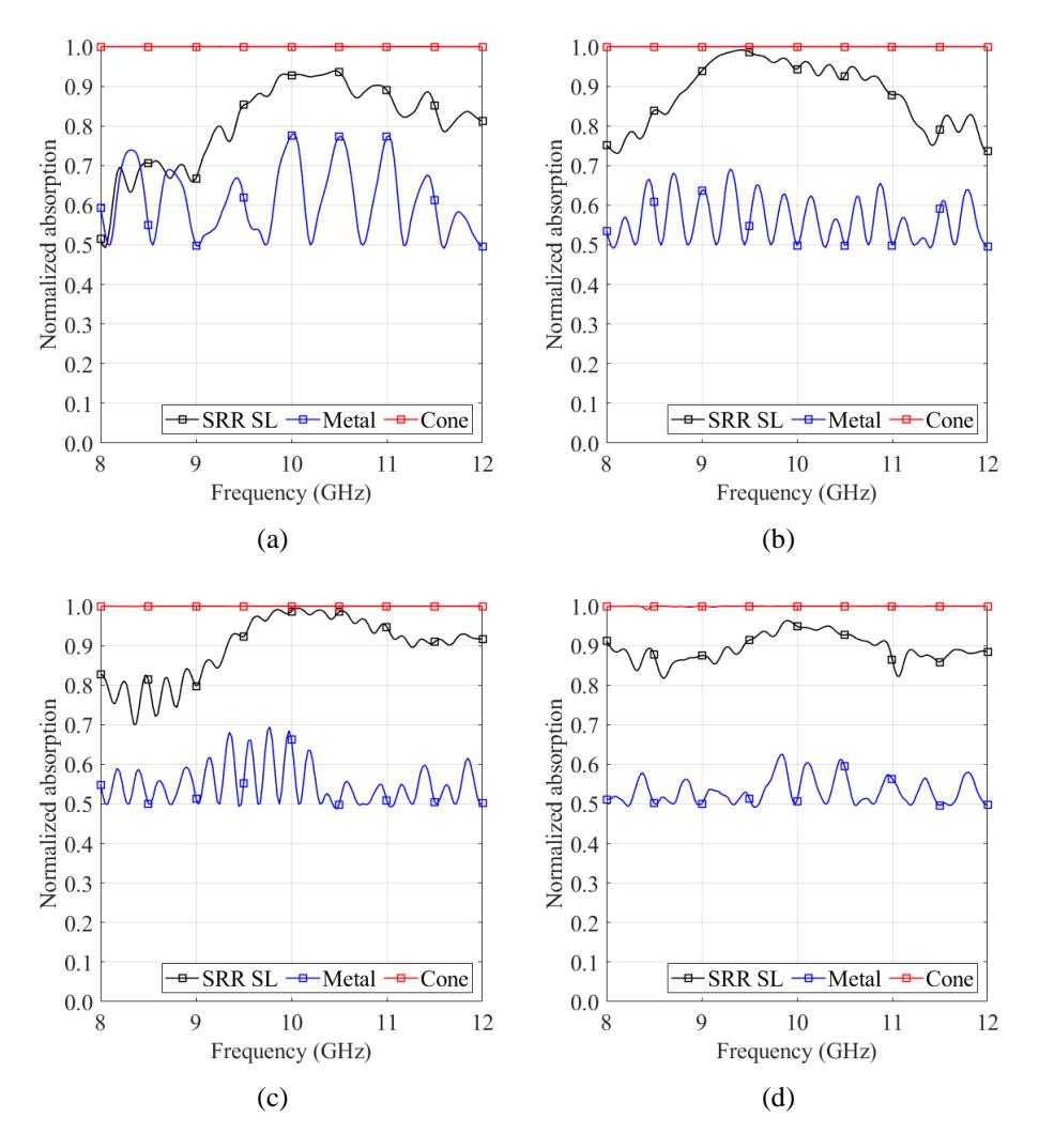
Figure 11 Measurement of open space characterization using designated scenarios and distances at an antenna orientation of ° : (a) 250 mm, (b) 500 mm, (c) 750 mm, (d) 1,000 mm.
The performance comparison among the measurement distances and antenna orientations for SRR and stripline are shown in Figure 12, where the performance of the SRR with stripline had a narrower bandwidth at the 0° and 45° antenna orientations than the 90° antenna orientations.
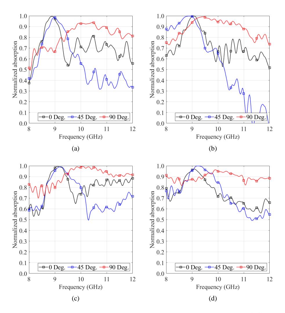
Figure 12 Measurement of open space characterization for SRR with stripline at designated distances: (a) 250 mm, (b) 500 mm, (c) 750 mm, (d) 1,000 mm.
The bandwidth of normalized absorption was 0.52 GHz for both antenna orientations of 0° and 45° with the center frequency of absorption shifting 1.47% from 8.85 GHz, while the bandwidth of normalized absorption was 0.77 GHz for an antenna orientation of 90° with the center frequency not at its highest normalized absorption, i.e., 0.94 at a frequency of 10.45 GHz. Besides the shift of the frequency center, there was also a degradation of the maximum absorption for the changes of antenna orientation at measurement distances of 250 mm as plotted in Figure 12(a).
These performances had a similar trend as the measurement distances of 1,000 mm as described in Figure 12(d). The maximum normalized absorption shifted 1.65% from the frequency center of 9.10 GHz with a maximum normalized absorption of 0.97 to 0.99 at antenna orientations of 0° and 45°, respectively. Meanwhile, at an orientation of 90° antenna, the maximum normalized absorption was 0.96 at a frequency of 9.90 GHz, i.e., not at its center frequency. The bandwidth for an antenna orientation of 90 degrees was 1.52 GHz and it decreased 55.26% and 36.18% for antenna orientations of 0° and 45°, respectively.
The performance for measurement distances of 500 mm and 750 mm had similar trends, as can be seen in Figures 12 (b) and 12(c), where the maximum normalized absorption was 0.99 for both measurement distances at antenna orientations of 0° and 45°. Furthermore, the bandwidth of normalized absorption increased with the change of antenna orientation to 90°, i.e., 2.05 GHz and 1.90 GHz, for measurement distances of 500 mm and 750 mm, respectively.
The X-band wave absorber formed by SRR with stripline achieved absorption with the experimental characterization using two horn antennas as transmitter and receiver in a free space measurement. The fully absorbent material structured as a cone, measured at a measurement distance of 250 mm, 500 mm, 750 mm, and 1,000 mm, perfectly absorbed the incident EM wave with the value of normalized absorption at 1. This condition represents an ideal absorption, although there are some factors that can fade the incident EM wave, such as loss of propagation.
Furthermore, for the metal plate with dimensions of 278.4 mm × 278.4 mm and measured with the same measurement distances of 250 mm, 500 mm, 750 mm, and 1,000 mm, the normalized absorption maximally fluctuated around 0.70 at a measurement distance of 250 mm, which was the maximum absorption the metal plate could achieve. The fluctuation of normalized absorption of the metal plate decreased along with the alteration of the measurement distance, which shows there is an influence of propagation loss and irradiated surface area, where the beam of the horn antenna will decrease along with the increase of the measurement distance. The beam of the horn antenna is assumed to weaken and the reflected EM wave become fainter as the distance moves to 500 mm, 750 mm, and 1,000 mm.
The absorption of the metal plate was used as a factor to normalize the absorption power of the DUT since it had the same size, distance, and measurement settings, and the absorption factor can only be affected by the DUT's structure or pattern. The SRR with stripline as X-Band wave absorber could absorb the EM wave with an average normalized absorption bandwidth of 0.61 GHz, 0.76 GHz, and 1.56 GHz, with the antenna orientation changing from 0°, 45°, to 90°, respectively. The increment of normalized absorption bandwidth with an antenna orientation of 90° was also marked by a decrease of the normalized absorption, which shows the design has asymetric performance in response to changes in antenna orientation because of the difference between the EM wave incident angle and the stripline orientation. The linear excitation of a horn antenna should be fully parallel with the stripline to achieve perfect absorption in the expected frequency region.
5 Conclusions
A model, the design, and implementation of an X-band metasurface absorber was presented and characterized using two horn antennas for distances of 250 mm, 500 mm, 750 mm, and 1,000 mm, and for 0°, 45°, and 90° antenna orientations. The model was constructed with two layers of dielectric substrate with an air spacing clamp and it was designed as a unit cell with SRR on top of the first dielectric layer and the stripline on top of the second dielectric layer. It was designed in a 3D simulation tool and approached with theoretical transmission lines with the same frequency response as the respective patch impedances and dimensions of the model. For verification of the single unit cell design, a model of the metasurface EM wave absorber was created with a finite array, providing an adequate frequency response in a single cell simulation. The implementation used a measurement method with two horn antennas as tranmitter and receiver and the DUT installed on a fully absorbent material in front of the antennas. The characterization of the X-band wave absorber formed by SRR with stripline showed a frequency response shift in a frequency range of 8.80 GHz to 9.25 GHz for an antenna orientation of 0° and 45°. The bandwidth of normalized absorption widened at an antenna orientation of 90° compared to an orientation of 0° and 45°. These conditions prove that the SRR and stripline could perform absorption in the X-band frequency range although it showed asymetrical performance with difference in antenna orientation.