

Abstrak
Suata Pendekatan Baru Untuk Analisis Arus-Arus Inverter
Dalam makalah ini dipresentasikan, Suatu pendekatan baru untuk analisis arus rata-rata dan rms pada komponen-komponen switching inverter dan nilai rms riak arus masukan inverter. Pendekatan yang diusulkan berbasis pada peluang komponen-komponen switching inverter menerima sinyal ON yang didapatkan dari nilai rata-rata tegangan fasa keluaran. Karena pengetahuan detil tentang pola switching inverter tidak diperlukan, metoda yang diusulkan sangat cocok untuk analisis arus-arus pada inverter dengan pola switching yang tidak bisa ditentukan. Untuk menunjukkan luasnya daerah penerapan, persamaan-persamaan arus rata rata dan rms komponen switching dan nilai rms riak arus masukan dari inverter yang menggunakan pengendali arus jenis hysteresis dan yang menggunakan pengendali PWM diturunkan. Hasil pengukuran disertakan untuk menunjukkan validitas metoda yang diusulkan.
Kata Kunci: Inverter, peluang sinyal ON, arus arus komponen, riak arus masukan.
1 Introduction
In inverter design, it is very important to know the average and rms currents in the switching devices and the rms value of the ripple component of the input current. The inverter switching devices can not be specified properly without knowing the average and rms currents in inverter switching devices. Information on the switching device currents is also useful for conduction loss analysis. Information on the rms value of the ripple component of inverter input current is important to specify the ripple current rating of the defilter capacitor.
In the cases of PWM inverters having switching function that can be predetermined, several analysis methods were proposed[1-6]. In [1-3], the PWM inverter currents were analyzed based on the Fourier series of the inverter switching function. The method, therefore, can not be applied when the inverter switching function can not be predetermined as in the case of inverter having
hysteresis discrete-pulse current Moreover, accurate results can not be obtained without taking into account a high number of harmonics with the associated complex additions and multiplications. In [4-5], the average and rms currents in the switching devices of PWM inverters were analyzed based on the duty factor of the inverter switching devices, that is, the ratio of the switching device ON time interval to the sum of the switching device ON and OFF time intervals of two consequtive ON and OFF signals. In samplingbased PWM inverters, this duty factor varies following the voltage reference signal. In inverter having hysteresis or discrete-pulse current controllers, however, there are no voltage reference signal nor regularity in the switching pattern and, therefore, the duty factor method can not be applied. At present, the switching device currents in this type of inverter are usually calculated in a rather oversimplified manner [7-8]. In [6], an attempt to simplify the analysis of PWM inverter currents is reported. Empirical formulae to compute the average and ams currents in sinusoidal PWM inverters were derived from simulation results. The empirical nature of the derived formulae makes it difficult to apply them to other inverters having different controllers.
In this paper, a new approach to analysis of the average and rms currents in inverter switching devices and the rms value of the ripple component of inverter input current is proposed. This approach is based on the probability with which the inverter switching devices receive ON signals. By using the proposed approach, analyses of inverter currents can be unified without the need of knowing the exact switching function of the inverter switching devices. Thus, the proposed approach is especially useful for inverters in which the exact switching functions can not be predetermined. To show the general applicability of this method, the expressions for the average and rms currents in switching devices and the rms value of the ripple component of input current of hysteresis current-controlled and PWM inverters are derived. Application of the probability method results in simple expressions to calculate the average and rms currents in inverter switching devices and the rms value of the ripple component of inverter input current.
The experimental results on three-phase hysteresis current-controlled and sinusoidal PWM inverters are included to verify the validity of the proposed method. The proposed method of analysis eliminates the time consuming simulation to calculate the inverter currents.
2 Analysis of inverter currents
In this section, the concept of probabilities of inverter switching devices receiving ON signals is introduced. This concept is used to generalize the analysis of average and rms currents of inverter switching devices and the ripple component of inverter input current. The detailed application of the proposed method to three-phase hysteresis current-controlled and PWM inverters are discussed in the next sections.
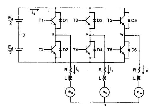
Figure 1 Three-phase inverter
2.1 Probabilities of inverter switching devices receiving ON signals
Fig. 1 shows the scheme of three-phase inverter which is used in this investigation. In order to calculate the inverter currents, the switching pattern or the instants when the switching devices receive ON signals should be known. In a sampling-based PWM inverter, the switching pattern of the switching devices can usually be predetermined. In a hysteresis current-controlled inverter, however, the switching instants of the switching power devices are determined by comparing the output and reference currents in a hysteresis comparator. Fig. 2 shows the simulated results of the phase-to-dc midpoint voltage vuo (which is similar to the base drive signal of the transistor T1) and the associated output phase current. This figure shows that the switching pattern of this type of inverter is irregular unlike the case of a sampling-based PWM inverter. Thus, we can not determine in advance the exact instants when the inverter switching devices receive ON
In this paper, a concept of probability to determine the chances when a switching device receives ON signals is
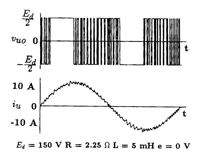
Figure 2 Simulated results of hysteresis current-controlled inverter. (a) Phase-to-dc midpoint voltage. (b) Output phase current
introduced to solve such a problem. Let us consider the upper-arm transistor (T1) and lower-arm transistor (T2) of phase u of the inverter in Fig. 1. When the average value (average over a short period) of the phase-to-dc midpoint voltage \(v_{uo}\), which is denoted by \(\overline{v}_{uo}\), is zero, then the probabilities of transistors T1 and T2 receiving ON signals are the same, that is,
\[P_{T1ON} = P_{T2ON} = \frac{1}{2} \tag{1}\] where \(P_{T1ON}\) and \(P_{T2ON}\) are the probabilities of transistors T1 and T2 receiving ON signals, respectively.
When the average value of the phase-to-dc midpoint voltage \(\overline{v}_{uo}\) is E<sub>d</sub>/2, which is the maximum value of \(\overline{v}_{uo}\), then the probabilities of transistors T1 and T2 receiving ON signals must be
\[P_{T1ON} = 1 \text{ and } P_{T2ON} = 0\] (2)
If the above discussion is generalized, the probabilities of transistors T1 and T2 receiving ON signals when the average value of the output voltage is \(\bar{v}_{\mu\alpha}\) are given by
\[P_{TION} = \frac{1}{2} + \frac{1}{2} \frac{\overline{v}_{uo}}{E_d / 2} \tag{3}\]
\[P_{T2ON} = \frac{1}{2} - \frac{1}{2} \frac{\overline{v}_{uo}}{E_{\perp}/2} \tag{4}\]
Similarly, the probabilities of inverter switching devices in the other two phases receiving ON signals can be determined based on the average value of the associated phase-to-dc midpoint voltages, that is,
\[P_{T3ON} = \frac{1}{2} + \frac{1}{2} \frac{\overline{v}_{VO}}{E_{\perp}/2} \tag{5}\]
\[P_{T4ON} = \frac{1}{2} - \frac{1}{2} \frac{\overline{v}_{VO}}{E_d / 2} \tag{6}\]
\[P_{TSON} = \frac{1}{2} + \frac{1}{2} \frac{\bar{v}_{WO}}{E_d / 2} \tag{7}\]
\[P_{76ON} = \frac{1}{2} - \frac{1}{2} \frac{\overline{v}_{WO}}{E_d / 2} \tag{8}\]
It should be noted that although eqns. (3)-(8) have similar form to the duty factor equations as those used in [4-5], the meaning of eqns. (3)-(8) are different to the duty factor equations. Eqns. (3)-(8) result in the probabilities of the inverter switching devices receiving ON signals at any instant of time. On the other hand, the duty factor equations result in the ratio of the inverter switching devices ON time interval to the sum of ON and OFF time intervals of two consequtive ON and OFF signals. The probabilities of the inverter switching devices receive ON signals can be obtained based on the average value of the phase-to-dc midpoint voltages even if the exact switching pattern is unknown as in the case of hysteresis current-controlled inverters. Moreover, these probability functions can also be used to determine the probabilities of various states of inverter. As an example, we can determine the probability of an inverter state in which the switching devices T1, T3. and T5 simultaneously receiving ON signals based on the probabilities of switching devices T1, T3, and T5 receiving ON signals. As will be demonstrated later, the probabilities of various states of inverter can be determined without the need of knowing the detailed swithing pattern. On the other hand, the duty factors of various states of inverter can not be determined simply based on the duty factors of the inverter switching devices.
2.2 Average and RMS currents of inverter switching devices
The output current of inverter in Fig. 1, \(i_u\) for example, will flow through transistor T1 when the transistor receives an ON signal and the current \(i_u\) is positive. When the current is positive but the transistor T1 receives an OFF signal (i.e., transistor T2 receives an ON signal), the current will flow through the lower diode D2. The currents that flow through transistor T1 and diode D2, therefore, can be obtained as
\[i_{T1} = P_{T1ON} \cdot i_u \tag{9}\]
\[i_{D2} = P_{T2ON} \cdot i_u \tag{10}\]
Squared values of transistor and diode currents, which are important for rms value calculation, are obtained as
\[i_{T1}^2 = P_{T1ON} \cdot i_u^2 \tag{11}\]
\[i_{D2}^2 = P_{T2ON} . i_u^2 (12)\]
The above equations are valid only when the current \(i_u\) is positive.
Assuming that the switching frequency is high, the inverter output current can be regarded as sinusoidal, and the phase u current for example, can be written as
\[i_{u} = \sqrt{2} I_{l} \sin \left(\theta - \varnothing\right) \tag{13}\] where \(I_l\) and \(\emptyset\) are the rms value and the power factor angle of the fundamental output current. The angle \(\theta\) is equal to \(\omega_t\) in which \(\omega_r\) and t are the fundamental angular frequency and time, respectively. The average and rms currents that flow through transistor T1 and diode D2 can be obtained as
\[I_{T1,av} = \frac{1}{2\pi} \int_{\phi}^{\pi+\phi} P_{T1ON} . i_{u} d\theta\] (14)
\[I_{T1,rms} = \sqrt{\frac{1}{2\pi} \int_{\phi}^{\pi+\phi} P_{T1ON} \cdot i_u^2 d\theta}\] (15)
\[I_{D2,av} = \frac{1}{2\pi} \int_{\phi}^{\pi+\phi} P_{T2ON} \cdot i_{u} d\theta\] (16)
\[I_{D2,rms} = \sqrt{\frac{1}{2\pi} \int_{\phi}^{\pi+\phi} P_{T2ON} \cdot i_u^2 d\theta}\] (17)
43 Rip. is a more of inverter input current
In general, the relationship among the output currents, input out end, and switching reads of inverter can be written as follow:
\[T_{i_1} = i_{i_1} t_{i_2} + i_{i_3} t_{i_4} + N_{i_3} t_{i_4} \tag{18}\]
hare \(s_u\), \(s_v\) and \(s_w\) are switching states of phase u, v, and w, respectively. The value of switching state of a phase is unity (zero) if the upper-arm switching device of that phase is receiving an ON (OFF) signal. Table I shows the summary of the relationship among the inverter input current, output currents, and the states of switching devices.
From eqn. (18) and Table 1, the inverter input current can only be calculated if we know the probabilities or the duty factor of eight possible states as shown in Table 1. In this case, however, we can not determine the duty factors of eight possible states of Table 1 based on the duty factors of each switching devices only. In order to calculate the duty factors of each possible states in Table 1, we need to know the detailed relationships among the ON and OFF signals or the exact switching patterns of all inverter switching devices. This task is very difficult (if not impossible) when the three phases of inverter are controlled independently as in the case of hysteresis current-controlled inverters. By using the proposed probability concept, however, the probabilities of each possible state in Table 1 can be calculated without the need of knowing the detailed switching patterns of inverter switching devices. The proposed probability method can still be applied even if the three phases of inverter are controlled independently.
From eqn. (18) and Table 1, the mean square value of inverter input current can be calculated as
\[I_d^2 = (P_4 + P_5) i_w^2 + (P_3 + P_6) i_v^2 + (P_6 + P_7) i_w^2\] (19)
Table 1. The average value of the above result over one fundamental period of the output current can be calculated as
\[I_{d,\alpha}^2 = \frac{1}{2} \int_0^{2\pi} I_d^2 d\theta\] (20)
Assuming no fosses in inverter, the input power and putput power of the inverter are equal, that is,
\[\mathcal{L}_{dl_A} = \sqrt{3} V_{ll} l_l \cos \phi \tag{21}\] where \(l_{H}\) is the rms value of the fundamental component of the output line-to-line voltages. Therefore, the decomponent of the inverter input current can be obtained as
\[I_{dc} = \frac{\sqrt{3}V_{il}}{E_d} I_l \cos \phi = \frac{3}{2\sqrt{2}} k I_l \cos \phi\] (22)
where
\[k = \frac{V_m}{E_d/2} \tag{23}\] in which \(V_m\) is the amplitude of the fundamental component of the output line-to-neutral voltages. Finally, the rms value of the ripple component of inverter input current can be calculated as
\[\widetilde{I}_{d} = \sqrt{I_{d,av}^2 - I_{u}^2} \tag{24}\]
Table 1 Relation among the inverter input current, output currents, and state of switching devices
| No | T1 | T2 | тз | T4 | T5 | Т6 | ĺď |
|---|---|---|---|---|---|---|---|
| 1 | OFF | ON | OFF | ON | OFF | ON | 0 |
| 2 | ON | OFF | OFF | ON | OFF | ON | iu |
| 3 | ON | OFF | OFF | ON | ON | OFF | -iv |
| 4 | OFF | ON | OFF | ON | ON | OFF | Íw |
| 5 | OFF | ON | ON | OFF | ON | OFF | ju |
| 6 | OFF | ON | ON | OFF | OFF | ON | iv |
| 7 | ON | OFF | ON | OFF | OFF | ON | −iw |
| 8 | ON | OFF | ON | OFF | ON | OFF | 0 |
3 Hysteresis current-controlled inverters
A current-controlled inverter is commonly used in high-performance ac motor drives and power supplies. In these applications hysteresis controller is commonly used as the current controller because of its simplicity to realize, fast response, and capability of limiting current. In hysteresis current-controlled inverters, the ON and OFF signals for the switching devices are determined based on comparison between the reference and actual output currents using a hysteresis comparator. Thus, the exact switching instants of each switching device can not be predetermined. In this section, the analysis method which has been developed in the previous section is applied to three-phase hysteresis current-controlled inverters.
3.1 Probabilities of 'nverter switching devices receiving ON signals
Though three independent hysteresis comparators are usually employed to control the three output phase currents, interaction between phases will occur when the neutral of load is isolated. This interaction occurs
because the sum of the three phase currents must always be zero. The effects of isolated neutral in the operation of hysteresis current-controlled inverters has been well explained and modeled by McMurray[9] and therefore, only the result is presented here.
When the neutral of load is isolated, current control in any phase can be done by controlling currents in the other two phases and therefore, one of the current controllers become redundant. The controller which is redundant is the one which is associated with the phase voltage having the greatest amplitude. The average value of the phase-to-dc midpoint voltages of the inverter become as shown in Fig. 3. It should be noted that although the average value of phase-to-dc midpoint voltages are nonsinusoidal, the average value of phaseto-neutral voltages are still sinusoidal. The expression for this voltage waveform, \(\overline{\upsilon}_{uo}\) for example, can be written as
\[\overline{v}_{uo} = \frac{E_d}{2} \times \begin{cases} \sqrt{3}k \sin(\theta + \frac{\pi}{6}) - 1 & \text{if } 0 \le \theta \le \frac{\pi}{3} \\ 1 & \text{if } \frac{\pi}{3} \le \theta \le \frac{2\pi}{3} \\ \sqrt{3}k \sin(\theta - \frac{\pi}{6}) - 1 & \text{if } \frac{2\pi}{3} \le \theta \le \pi \\ \sqrt{3}k \sin(\theta + \frac{\pi}{6}) + 1 & \text{if } \pi \le \theta \le \frac{4\pi}{3} \\ -1 & \text{if } \frac{4\pi}{3} \le \theta \le \frac{5\pi}{3} \\ \sqrt{3}k \sin(\theta - \frac{\pi}{6}) + 1 & \text{if } \frac{5\pi}{3} \le \theta \le 2\pi \end{cases} (25)\]
The maximum value of k is \(2/\sqrt{3}\). The expressions for \(\overline{v}_{vo}\) and \(\overline{v}_{wo}\) are similar to eqn. (25) but with the phase displacements of \(2\pi/3\) and \(4\pi/3\), respectively.
Based on the average value of phase-to-dc midpoint voltages of the inverter, the probabilities of inverter switching devices receiving ON signals can be determined. Probabilities of transistors T1 and T2 receiving ON signals can be obtained by substituting eqn.(25) into eqns. (3)-(4) and the results are
\[P_{\text{TION}} = \begin{cases} \frac{\sqrt{3}}{2} \, \mathbf{k} \sin(\theta + \frac{\pi}{6}) & \text{if } 0 \le \theta \le \frac{\pi}{3} \\ 1 & \text{if } \frac{\pi}{3} \le \theta \le \frac{2\pi}{3} \\ \frac{\sqrt{3}}{2} \, \mathbf{k} \sin(\theta - \frac{\pi}{6}) & \text{if } \frac{2\pi}{3} \le \theta \le \pi \\ \frac{\sqrt{3}}{2} \, \mathbf{k} \sin(\theta + \frac{\pi}{6}) + 1 & \text{if } \pi \le \theta \le \frac{4\pi}{3} \\ 0 & \text{if } \frac{4\pi}{3} \le \theta \le \frac{5\pi}{3} \\ \frac{\sqrt{3}}{2} \, \mathbf{k} \sin(\theta - \frac{\pi}{6}) + 1 & \text{if } \frac{5\pi}{3} \le \theta \le 2\pi \end{cases}\](26)
\[P_{T2ON} = \begin{cases} 1 - \frac{\sqrt{3}}{2} k \sin(\theta + \frac{\pi}{6}) & \text{if } 0 \le \theta \le \frac{\pi}{3} \\ 0 & \text{if } \frac{\pi}{3} \le \theta \le \frac{2\pi}{3} \\ 1 - \frac{\sqrt{3}}{2} k \sin(\theta - \frac{\pi}{6}) & \text{if } \frac{2\pi}{3} \le \theta \le \pi \\ -\frac{\sqrt{3}}{2} k \sin(\theta + \frac{\pi}{6}) & \text{if } \frac{2\pi}{3} \le \theta \le \pi \\ 1 & \text{if } \frac{4\pi}{3} \le \theta \le \frac{5\pi}{3} \\ -\frac{\sqrt{3}}{2} k \sin(\theta - \frac{\pi}{6}) & \text{if } \frac{5\pi}{3} \le \theta \le 2\pi \end{cases}\] \[V_{T1,rms} = I_{l} \sqrt{\frac{\pi - \phi}{6\pi} + \frac{\sqrt{3} - 2k}{2\pi\sqrt{3}} \cos(\frac{\pi}{6} + 2\phi)}\] \[V_{T2ON} = \begin{cases} 1 - \frac{\sqrt{3}}{6\pi} k \sin(\theta + \frac{\pi}{6}) & \text{if } \frac{2\pi}{3} \le \theta \le \pi \\ 0 & \text{if } \frac{4\pi}{3} \le \theta \le \frac{5\pi}{3} \end{cases}\] \[V_{T1,rms} = I_{l} \sqrt{\frac{\pi - \phi}{2\pi} + \frac{2\sqrt{3}k - 3}{6\pi} \sin 2\phi}\] \[V_{T1,rms} = I_{l} \sqrt{\frac{\pi - \phi}{2\pi} + \frac{2\sqrt{3}k - 3}{6\pi} \sin 2\phi}\]
Similarly, the probabilities of the other transistors receiving ON signals can be obtained based on the average value of the phase-to-dc midpoint voltage of the associated phases.
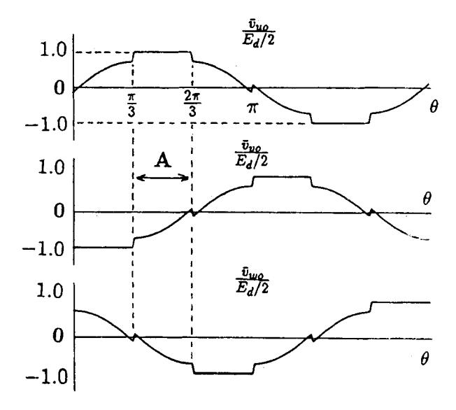
Figure 3 Waveforms of average value of the output phase voltages of hysteresis current-controlled inverter.
3.2 Average and RMS currents of inverter switching
The probabilities of transistors receiving ON signals as given by eqns. (26)-(27) can be used to determine the average and rms values of currents in inverter switching devices. If the hysteresis band is very small compared to the amplitude of reference current, the inverter output current can be regarded as sinusoidal. Substituting eqns. (26)-(27) into eqns. (14)-(17) and performing the integration, the average and rms currents of transistor T1 and diode D2 can be obtained. The resulting expression for the average value of current in transistor T1 is
\[I_{T1,av} = \frac{I_l}{\pi\sqrt{2}} \left[ 1 + \frac{\pi}{4} k \cos \phi \right]\] (28)
and for the rms current is
\[I_{T1,rms} = I_l \sqrt{\frac{\pi + 3\phi}{6\pi} + \frac{\sqrt{3} - 2k}{2\pi\sqrt{3}}} \cos(\frac{\pi}{6} + 2\phi) + \frac{2k}{\pi\sqrt{3}} \cos(\frac{\pi}{6} + \phi)\] (29)
\[I_{T1,rms} = I_1 \sqrt{\frac{\pi - \phi}{2\pi} + \frac{2\sqrt{3}k - 3}{6\pi}\sin 2\phi}\] (30)
where \(\frac{R}{3} \le \beta \le \frac{R}{2}\). The resulting expression for the expression of the expression diode D2 is
\[I_{D2,ab} = \frac{l_1}{\sqrt{2}} \left[ i - \frac{\pi}{4} k \cos \phi \right]\] (31)
and for the ems carrent is
\[I_{D2, ms} = I_{l} \sqrt{\frac{2\pi - 3\phi}{6\pi} - \frac{\sqrt{3} - 2k}{2\pi\sqrt{3}} \cos\left(\frac{\pi}{6} + 2\phi\right) - \frac{2k}{\pi\sqrt{3}} \cos\left(\frac{\pi}{6} + \phi\right)}\] (32)
when \(0 \le \phi \le \frac{\pi}{3}\), and
\[I_{D2,rms} = I_1 \sqrt{\frac{\phi}{2\pi} - \frac{2\sqrt{3}k - 3}{6\pi}\sin 2\phi}\] (33)
when \(0 \le \phi \le \frac{\pi}{3}\)
Assuming the symmetrical operation of the inverter, the results for other transistors and diodes are the same.
3.3 Input current ripple
As stated earlier, the ON and OFF signals for the inverter switching devices are determined simply based on the direct comparison between the actual and reference currents. Because the controllers in the three phases of the inverter are working independently, the duty factors of each state in Table 1 can not be predetermined even if the duty factors of each inverter switching device are known. Thus, the duty factor method can not be applied to this analysis. By using the proposed probability concept, however, we can determine the probabilities of each state in Table 1 based on the probabilities of inverter switching devices receiving ON signals. The results can be used to determine the inverter input current ripple as we will show in the following.
In the interval A of Fig. 3, the transistor T1 is idle and locks the line of phase u into the positive bus of dc supply. During this interval, the inverter output currents are controlled by transistors in phases v and w. Thus, the possible states during the interval A are state numbers 2, 3, 7, and 8 of Table 1. The probabilities of the other states are zero. Therefore, the mean square value of the inverter input current can be obtained as
\[I_d^2 = P_2 i_u^2 + P_3 i_v^2 + P_7 i_w^2\] (34)
Because the probabilities of transistors T3, T4, T5, and T6 receiving ON signals are known then the probabilities of state numbers 2, 3, and 7 can be calculated, that is,
\[P_2 = P_{I4ON} \times P_{I6ON}\]
\[=\frac{\sqrt{3}}{2}k\sin(\theta+\frac{\pi}{6})\times\frac{\sqrt{3}}{2}k\sin(\theta-\frac{\pi}{6})\] (35)
\(P_3 = P_{T4ON} \times P_{T5ON}\)
\[= \frac{\sqrt{3}}{2} k \sin(\theta + \frac{\pi}{6}) \times \left[ 1 - \frac{\sqrt{3}}{2} k \sin(\theta - \frac{\pi}{6}) \right]\] (36)
\(P_7 = P_{T3ON} \times P_{T6ON}\)
\[= \left[1 - \frac{\sqrt{3}}{2}k\sin(\theta + \frac{\pi}{6})\right] \times \frac{\sqrt{3}}{2}k\sin(\theta - \frac{\pi}{6})\] (37)
Substituting eqns. (35)-(37) into eqn. (34) and assuming that the inverter output currents are sinusoidal the following equation is obtained
\[I_{d}^{2} = 2I_{l}^{2} \sin^{2}(\theta - \phi) \times \frac{\sqrt{3}}{2} k \sin(\theta + \frac{\pi}{6}) \times \frac{\sqrt{3}}{2} k \sin(\theta - \frac{\pi}{6})\] \[+ 2I_{l}^{2} \sin^{2}(\theta - \frac{2\pi}{3} - \phi) \times \frac{\sqrt{3}}{2} k \sin(\theta + \frac{\pi}{6}) \times \left[1 - \frac{\sqrt{3}}{2} k \sin(\theta - \frac{\pi}{6})\right]\] \[+ 2I_{l}^{2} \sin^{2}(\theta - \frac{2\pi}{3} - \phi) \times \frac{\sqrt{3}}{2} k \sin(\theta + \frac{\pi}{6}) \times \left[1 - \frac{\sqrt{3}}{2} k \sin(\theta - \frac{\pi}{6})\right]\](38)
The average value of the above equation over the interval A of Fig. 3 can be calculated as
\[I_{d,av}^{2} = \frac{3}{\pi} \int_{\pi/3}^{2\pi/3} i_{d}^{2} d\theta\] \[= \frac{3}{2\pi} k I_{1}^{2} \left[ 3 - \cos 2\phi - \frac{k\pi}{8} (1 - 2\cos 2\phi) - \frac{3\sqrt{3}k}{8} (1 - \frac{3}{2}\cos 2\phi) \right]\](39)
Because of the symmetrical operation of the inverter, the results for other sixty degrees periods are the same. Finally, the rms value of the ripple component of inverter input current can be obtained by substituting eqn. (39) into eqn. (24) and the result is
\[\text{[rumus tidak dapat ditampilkan dengan baik — lihat PDF asli]}\] (40)
4 PWM inverters
A PWM inverter is commonly used in ac drives and UPS. A lot of PWM techniques were proposed in the literature. In this section, the inverter current analysis method which has been developed in the previous section is applied to three-phase PWM inverters.
4.1 Probabilities of inverter switching devices receiving ON signals
Regardless of the employed PWM technique, the main purpose of the PWM technique is to control the pulsewidth of the inverter output voltage so that the average value of the output voltage is equal to the desired pattern or reference signal. In the case of sinusoidal PWM inverters, the average value of the phase-to-dc midpoint voltage will be sinusoidal as shown in Fig. 4. The phase u voltage, for example, can be written as
\[\frac{\overline{v}_{uo}}{E_d/2} = k \sin \theta \tag{41}\]
The maximum value of k is unity.
Substituting eqn. (41) into eqns. (3)-(4), the probabilities of transistors T1 and T2 receiving ON signals can be obtained as
\[P_{T1ON} = \frac{1}{2} + \frac{1}{2}k\sin\theta \tag{42}\]
\[P_{T2ON} = \frac{1}{2} - \frac{1}{2}k\sin\theta \tag{43}\]
Similarly, the probabilities of the other transistors receiving ON signals can be obtained based on the average value of the phase-to-dc midpoint voltage of the associated phases.
Figure 4 Waveforms of average value of the output phase voltages of sinusoidal PWM inverter.
4.2 Average and RMS currents of switching devices
Substituting eqns. (42)-(43) into eqns. (14)-(17) and performing the integral operation, the expressions for average and rms currents in T1 and D2 are obtained. The resulting expressions for transistor T1 are
\[I_{T1,av} = \frac{I_I}{\pi\sqrt{2}} \left[ 1 + \frac{\pi}{4} k \cos \phi \right]\] (44)
\[I_{T1,rms} = I_l \sqrt{\frac{1}{4} + \frac{2}{3\pi} k \cos \phi}\] (45)
and the resulting expressions for diode D2 are
\[I_{D2,av} = \frac{I_l}{\pi\sqrt{2}} \left[ 1 - \frac{\pi}{4} k \cos \phi \right] \tag{46}\]
\[I_{D2,rms} = I_l \sqrt{\frac{1}{4} - \frac{2}{3\pi} k \cos \phi}\] (47)
Assuming the symmetrical operation of the inverter, the results for other transistors and diodes are the same as those obtained above. Extension of this analysis to the case of nonsinusoidal reference signals is straightforward. The proposed method can also be applied to the cases when the PWM signals are generated in random fashion as used in [11].
4.3 Input Current Ripple
Regardless of the employed PWM technique, a well designed PWM inverter should conform the pulse consistency rule as introduced in [10]. The rule says that the pulses of the output line-to-line voltage should have the same polarity through an entire half-period of the output fundamental period. All the pulses should be positive for the positive half-period and should be negative for the negative half-period of the output lineto-line voltage. In the interval B of Fig. 4, for example, the pulses of line-to-line voltages vuv , vuw , and vwv should be positive. This means that in this interval, transistor T3 of inverter in Fig. 1 will receive ON signal only when transistor T5 receives ON signal and, both transistors T3 and T5 will receive ON signals only when transistor T1 receives ON signal. The relationships among the probabilities of transistors T1, T3, and T5 receiving ON signals are shown in Fig. 5. Thus, the possible states during the interval B of Fig. 4 are state numbers 1, 2, 3, and 8 of Table 1. As it is shown in Table 1, the inverter input current during state numbers 1 and 8 is zero.
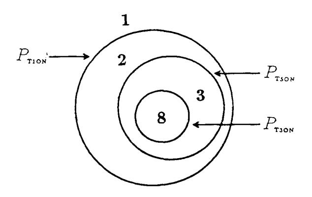
Figure 5 Relationships among the probabilities of the transistors T1, T3, and T5 receiving ON signals.
In state numbers 2 and 3, the inverter input current is equal to \(i_u\) and \(-i_v\), respectively. The probabilities of state numbers 2 and 3 can be calculated as
\[P_2 = P_{T1ON} - P_{T5ON}\]
\[=\frac{\sqrt{3}}{2}k\sin(\theta-\frac{\pi}{6})\tag{48}\]
\[P_3 = P_{TSON} - P_{T3ON}\]
\[=\frac{\sqrt{3}}{2}k\sin(\theta-\frac{\pi}{2})\] (49)
The probabilities of state numbers 4, 5, 6, and 7 are zero during the interval B. Thus, the mean square value of the inverter input current can be calculated as
\[I_d^2 = P_2 i_u^2 + P_3 i_w^2 (50)\]
Substituting eqns. (48)-(49) into eqn. (50) and by assuming that the inverter input currents are sinusoidal, the following equation is obtained
\[I_{d}^{2} = I_{l}^{2} \left[ 1 - \cos(2\theta - 2\phi) \frac{\sqrt{3}}{2} k \sin(\theta - \frac{\pi}{6}) + I_{l}^{2} \left[ 1 - \cos(2\theta + \frac{2\pi}{3} - 2\theta) \right] \frac{\sqrt{3}}{2} k \sin(\theta + \frac{\pi}{2}) \right]\] \[(51)\]
The average value of the above result over the interval B of Fig. 4 can be calculated as
\[I_{d,av}^{2} = \frac{3}{\pi} \int_{\pi/6}^{\pi/2} I_{d}^{2} d\theta\] \[= \frac{3\sqrt{3}}{2\pi} I_{l}^{2} \left[ 1 + \frac{2}{3} \cos 2\phi \right]\] (52)
Because the symmetrical operation of the inverter, the results over other sixty degrees periods are the same. Finally, the ripple component of the inverter input current is calculated by substituting eqn. (52) into eqn. (24) and the result is
\[\widetilde{I}_d = I_l \sqrt{k \left[ \frac{\sqrt{3}}{2\pi} + \left( \frac{2\sqrt{3}}{\pi} - \frac{9}{8} k \right) \cos^2 \phi \right]}\] (53)
It should be noted that except the assumptions that the average value of the line-to-line output voltages is sinusoidal and the pulse consistency rule is conformed, no further assumptions are used in the derivation of eqn. (52). Thus, as long as these two assumptions are justified, the result as given by eqn. (53) is valid for any PWM inverters. It is also interesting to note that the switching frequency has no influence on the rms value of the ripple component of inverter input current. Thus, we can not reduce this current ripple by increasing the switching frequency.
5 Experimental results
In order to verify the validity of the proposed analysis method, a three-phase inverter with the scheme as shown in Fig. 1 was constructed. Each leg of inverter was implemented by using a bipolar power transistor module. To avoid a short-circuit through the upper and lower transistors, a dead time of \(12\mu s\) was used in the control circuit. In this experiment, only static R-L loads were used. The experimental conditions are shown in Table 2.
Table 2 Experimental conditions
| Load | Ed(∀) | R(Ω | L(mH) | f, (Hz) |
|---|---|---|---|---|
| Α | 150 | 2.25 | 5 | 50 |
| В | 150 | 0.5 | 9 | 50 |
To measure the average and rms currents in inverter switching devices, the current that flowing through one pair of transistor and diode, for example T1 and D1, is measured simultaneously with the associated output phase current, that is, iu. The measurement was done by using a Hall current sensor and the waveforms are recorded by using a digital storage oscilloscope. The data in the oscilloscope is read and analyzed by a personal computer to compute the average and rms currents in transistor and diode. When both device and output phase currents are positive, then the device current is assumed be the transistor current and, when both the currents are negative to then the device current is equal to the diode current.
Figs. 6 and 7 show the calculated and experimental results of the average and rms currents in transistor and diode of three-phase hysteresis current-controlled inverter and sinusoidal PWM inverter, respectively. Switching frequency of 1.5 kHz and hysteresis band of 0.25 A were used in the sinusoidal PWM and hysteresis current-controlled inverteres, respectively. Good correlation between the experimental and calculated results can be appreciated from these figures.
Measurements of the ripple component of inverter input current were done by using a digital multimeter which has a capability of measuring the rms value of the ac component of a given signal. Figs. 8 and 9 shows the calculated and experimental results for the hysteresis current-controlled and sinusoidal PWM inverters, respectively. The figures show that the calculated results compare favorably with the experimental ones.
6 Conclusion
A new approach to analysis of average and rms currents in inverter switching devices and rms value of ripple
component of inverter input current has been presented and verified by experimental results. The proposed method is based on the probabilities of inverter switching devices receiving ON signals which can be obtained from the average value of phase-to-dc midpoint voltages. As long as the switching frequency is high, the proposed method can be applied to other types of inverters, which is left for future investigation. The proposed analytical method eliminates the time consuming simulation to evaluate the inverter currents
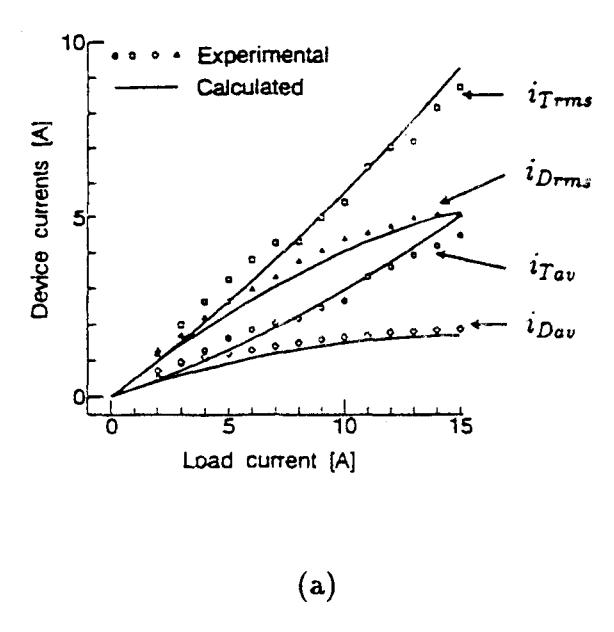
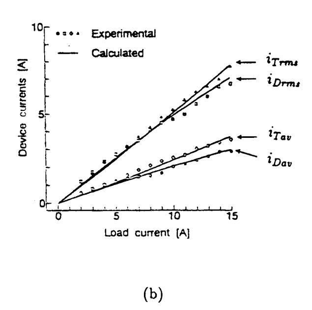
Figure 6 Average and rms currents in the switching devices of hysteresis current-controlled inverter. (a) Load A. (b) Load B.
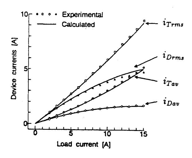
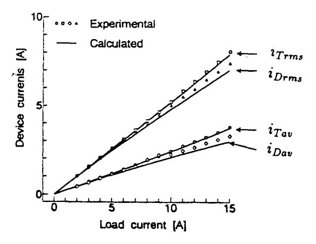
Figure 7 Average and rms currents in the switching devices of sinusoidal PWM inverters. (a) Load A. (b) Load B.
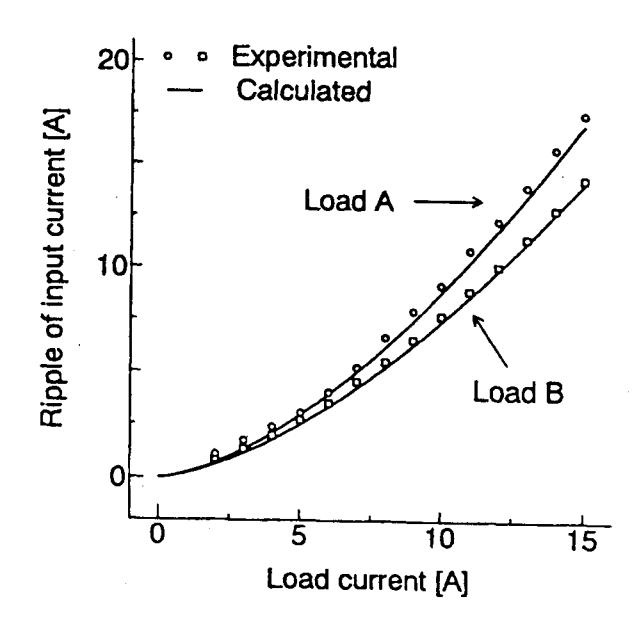
Figure 8 Ripple component of hysteresis current-controlled inverter input current.
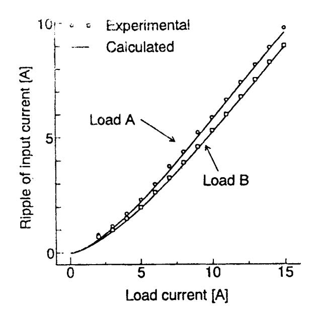
Figure 9 Ripple component of sinusoidal PWM inverter input current.
Acknowlegments
Part of this work has been supported by the Ministry of Research and Technology through RUT-V. Another part of this work has been done during the author stay in Tokyo Institute of Technology, Japan.