

Sari
Studi mengenai titik kuantum GaSb
Quantum Dot adalah material yang mempunyai struktur nano, yang merupakan objek untuk penelitian fumndamental maupun untuk penerapannya. Dalam makalah ini dilaporkan hasil-hasil yang pertama yang kita peroleh dalam pembuatan Quantum Dot dari GaSb dalam laboratorium kami. Quantum Dot ini telah ditumbuhkan dengan menggunakan penumbuhan yang "selforganized" dengan reaktor MOCVD dengan mempergunakan Trimetilgalium dan Trisdismetilantimonat sebagai sumber-sumber metalorganik dan GaAs digunakan sebagai substrat. Hasilnya ditelaah dengan menggunakan SEM. Telah disarahkan karakterisasi lanjutan yang harus dilakukan.
Kata kunci: MOCVD, GaSb, Titik kuantum.
1 1ntroduction
Quantum dots (QD) is of great physical interest, since its electronic structure lies between the band-structure and the discreet structure of the atom. The typical size of this transition is on the order of the de Broglie wavelength, which is of the order of tens of nm. The microcrystal have a band electronic structure, but for the dots, whoes size is on the order of tens of de Broglie wavelength may have a discreet electronic structure.
Quantum dots have been used to make lasers<sup>1</sup>, and infrared photo detectors<sup>2</sup>. It is also expected that QD also may serve as a Non-linear medium for Femtosecond Technology<sup>3</sup>.
QD can be prepared without using complicated lithography, namely by using the self-organized growth using MBE or MOCVD. We have carried out the preparation using a vertical home-made MOCVD. In self organized growth we make use of the mismatch between the 2 consecutive grown layers. The first observation of QD by self organized growth was carried out by Goldstein et.a1<sup>4</sup>. For GaSb, the growth of QD using MOCVD has been carried out by Goldys and Kinder<sup>5</sup>. We follow this method. In the near future we would like to characterize these QD using its electrical properties. In the next section we describe the experimental method. In sec.3, we describe the characterization of the obtain dots by observing its size distribution using Scanning Electron Microscope. In the same section we describe the characterization of the QD by measuring its electrical properties to be carried out in the near future and summarize our results obtained sofar.
2 GaSb quantum dot fabrication
For the fabrication of GaSb thin flims and QD we use our home built MOCVD reactor, which is a vertical reactor. The schematics of the reactor is shown in Fig. 1. As metal-organic (MO) source we use trimethylgallium (TMG) for Ga and trisdimethylaminoantimonate (TDMASb). We use purified hydrogen gas as carrier gas. In the first stage we grow GaSb and observe the optimal growth conditions, such as sample temperature, reactor gas pressure, flow-rate of the carrier gas and the III-V ratio, of the MO gasses. The resulting thin film is then evaluated by looking at the XRD pattern. The obtained GaSb film is considered reasonable if we obtain peaks only in the c-axis direction. A typical XRD pattern is shown in Fig. 2, where we observe only the (002) and (004) peaks.
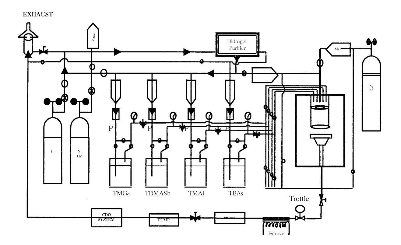
Figure 1 The schematics of the MOCVD reactor.
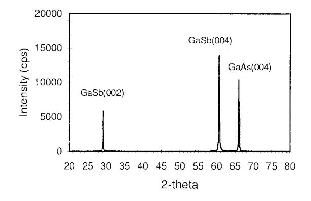
Figure 2 The X-ray diffraction pattern of GaSb film.
The next step is to grow the quantum dot. Its can be achieved by controlling the MO source flow, using the valve for the hydrogen gas which flows through the bubbler. The valve is replaced by a pneumatic valve. To turn on the valve we use pressurized Nitrogen and to turn off the valve we release the pressurized gas. Using this control system we can control the MO flow rapidly. The introduction and release the pressurized gas is controlled by an electromagnet. Therefore the control of the flow is fast. For the growth of the QD we have to be able to control the flow up to seconds.
3 Results and discussions
In this section we will present our preliminary results of the growth of the QD. The growth of QD, is carried out at different Ga/Sb flow ratio, the length of time the MO flows into the reactor and substrate temperature is maintained at 520° and 540°C. The SEM picture of the QD is shown in fig. 3 and the size (diameter) of the QD is summarized in Table 1.
Table 1 GaSb dots dimensions for various deposition parameter.
| Sam- ple | TMGa/T DMASb ratio (sccm/s ccm) | Growt h time (sec) | Sub strate tempe- rature (°C) | Diameter (nm) | Density (1013 m-2) | Interdotd istance (nm) |
|---|---|---|---|---|---|---|
| #1 | 1/1 | 20 | 520 | 55.6 | 0.92 | 222.2 |
| #3 | 3/3 | 20 | 520 | 64.2 | 0.98 | 185.1 |
| #5 | 3/3 | 60 | 520 | 148.1 | 1.01 | 150.0 |
| #7 | 3/3 | 40 | 540 | 148.1 | 2.37 | 148.1 |
The histogram of the QD size is shown in Fig. 4. The development of the QD size and the inter dot distance as the growth parameter is changed is illustrated in Fig. 5. As the growth time is increased the dot density does not increase significantly. The growth time has a more significant effect on the inter-dot distance and the dot size.
Figure 3 The SEM picture of the quantum dots
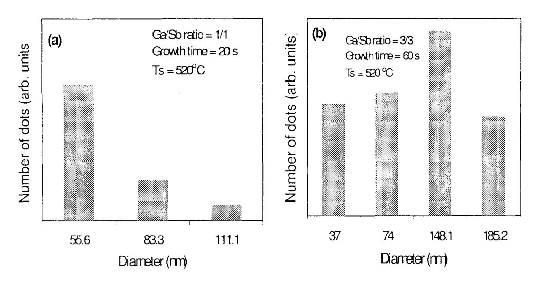
Figure 4 The histogram of the QD size of sample #1 (a) and sample #5 (b).
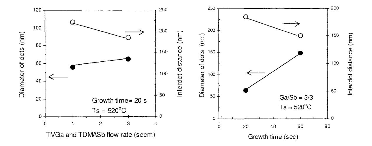
Figure 5a Diameter of GaSb dots and inter-dots distance as function of TMGa and TDMASb flow rate.
Figure 5b Diameter of GaSb dots and inter-dot distance as function of growth time.
At present we are still trying to improve the reactor to improve the results and to characterize further the QD. In the near future we would like to characterize the QD by measuring the electrical properties using C-V and DLTS measurements at different temperatures, florn Liquid Nitrogen temperatures; to room temperature. In these measurement the QD is considered as a "defect" and measure the charge density as function of depth as well as the defect level. For this propose the sample preparation is more complicated. We have to use n-type GaAs substrate, prepare the QD and prepare a cap layer and metalization on top of it. In this way we prepare the Schottky diode for the measurements of the electrical properties. The result of the measurement is to be compared with the same diode without QD.
4 Acknowledgment
This work was supported by The HTTP Program of URGE Project, The Ministry of National Education, The Republic of Indonesia, under contract No: 001 HTTP-IV/URGE/1999.
5 References
- Bimberg, D, Grundmann, M, Heirichsdorff, F, Ledentsov, NN, Ustinov, VM, Zukov, E, Kovsh, AR, Maximov, MV, Shemyakovv, YM, Volovik, BV, Tsatsulnikov, AF, Kopev, PS, & Alferov, ZhI, This Solid Films, 367, 235 (2000).
- 2. Towe, E, & Pan, D, IEEE J. Selected Topics Quantum Electron, 6, 408 (2000).
- 3. Ishikawa, Hiroshi in Femtosecond Technology, Kamia, T, Saito, F, Wada, O, Yajima Eds. Sringer 211 (1999).
- 4. Goldstein, L, Glass, F, Marzin, JM, Charasse, MN, & Le Roux, G, Appl. Phys. Lett., 47, 1099 (1985).
- 5. Goldys, EM, & Kinder, M, Appl. Phys. Letter, 73. 1233 (1998).