

Sari
Efek proses annealing terhadap sifat-sifat optik film tipis Zinc-Oxide (ZnO) yang ditumbuhkan dengan MOCVD
Telah dilakukan proses annealing pada film tipis ZnO untuk berbagai harga temperatur. Efek dari proses annealing terhadap sifat optik lapisan tipis ZnO ini dipelajari agar dapat diaplikasikan pada divias optoelektronik. Spektrum transmitansi optik telah diukur, dan diperoleh adanya penurunan spektrum transmitansi di daerah UV-Vis sejalan dengan diturunkannya temperatur annealing. Hal ini disebabkan oleh meningkatnya rapat pembawa muatan yang disebabkan oleh bertambahnya oxygen vacancies selama proses annealing pada temperatur 300°C. Ditemukan pula bahwa ujung absorpsi bergeser ke arah energi yang lebih rendah saat lapisan tipisnya di-annealed pada temperatur 300°C di udara.
Kata kunci: annealing, sifat optik, spektrum transmitansi, ZnO.
1 Introduction
ZnO is important electronic semiconductor material for applications to optoelectronic devices. It has large piezoelectric and optical coupling coefficients and films oriented along the c-axis are useful for optical wave guides and surface acoustic wave devices<sup>1,3</sup>. The electrical and optical properties of ZnO film depend strongly on the preparation conditions such as the substrate temperature. It has been shown in the literature that the heat treatment after preparation can also change the film properties.<sup>2,3)</sup>
The information of the optical properties of ZnO is indispensable for design and analysis of various optical and optoelectronic devices. In this paper ZnO film was deposited by metalorganic chemical vapor deposition (MOCVD) method because this method can give acceptable deposition rates at low temperature and potential large scale application. The aim of this paper is to show the influence of heat treatment on the optical properties of ZnO film.
2 Experimental
ZnO thin films were deposited on a corning 7059 glass substrate. Diethylzinc (DEZ) and H<sub>2</sub>O were used as reactant gas and were contained in bubbler. Purified Ar gas (99.999%) was used as the carrier gas. The flow rates of DEZ and H<sub>2</sub>O transported to the growth chamber were set to 27.8 and 18.4 µmol/min, respectively. The temperature of substrate was kept at 100°C and pressure at 1 torr during deposition for 10 min. The thickness of the deposited ZnO film was 2 µm. After the ZnO films were grown, they were annealed in Ar ambient at a pressure 1 torr and in air atmosphere for 30 min. The annealing temperature were varied from 100°C to 350°C. The optical transmittance measurement were carried out using UV-VIS spectrometer and the structural properties of the film were investigated by using x-ray difractometer
3 Result and discussion
The sheet resistivity of undoped and doped ZnO annealed in argon is shown in Fig. 1. The resistivity decreases as the annealing temperature is increased up to 150 °C and has a minimum value. The resistivity of doped ZnO does not change above this temperature, but the resistivity of undoped ZnO increases again. The decrease in resistivity may be caused by the oxygen desorption at the grain boundary<sup>4)</sup>. This may cause the annihilation of the trap states, resulting in the increase of carrier concentration.
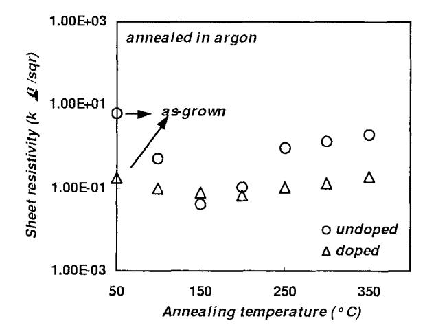
Figure 1 Sheet resistivity undoped and doped ZnO thin film vs annealing temperature in argon
Annealing in air causes the increase of the sheet resistivity of both the undoped and the doped ZnO thin film. At relatively low temperature (below 250°C) sheet resistivity increases. At this point, ionization oxygen vacancies may cause the increase of the surface states of the film. Above 250 °C this process saturates as shown in Fig. 2.
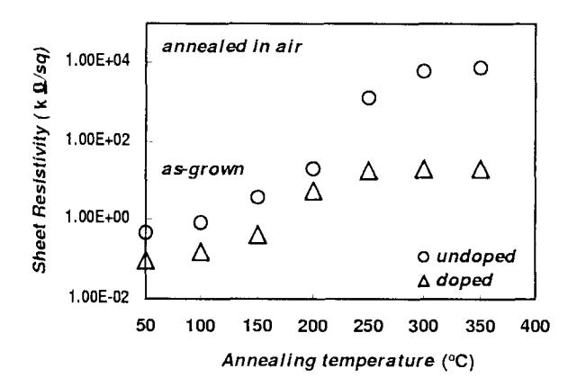
Figure 2 Sheet resistivity undoped and doped ZnO thin film vs annealing temperature in air
The effect of annealing treatment on optical properties of the ZnO undoped film is shown in Fig. 3. All the film exhibits a high transmittance in visible region and shows a sharp fundamental absorption edge. As a result of annealing treatment, it was also found the shift in the absorption edge to lower energy for undoped ZnO film annealed at \(300^{\circ}\)C in air. The optical band gap was estimated by plotting the relationship between the direct transition type, \((\alpha hv)^2\) vs hv using the optical transmittance spectra shown in Figs. 3 and 4.
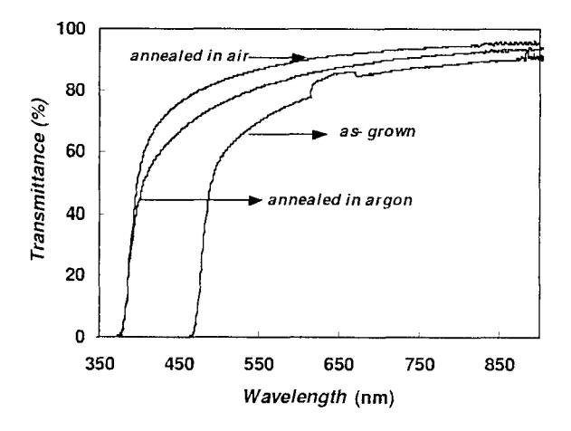
Figure 3 Optical transmittance of the undoped ZnO thin film
The estimated values of the band gap for all film are reported in Tab. 1. It is clear that the optical gap decreases when the undoped film is annealed in air, while for doped ZnO film, this phenomenon almost does not appear. Annealing treatment in argon at 300°C causes no change in optical band gap. This result is related to the fact that at this temperature the sheet resistivity is still the same as in as-grown film. The change in optical gap of ZnO films can be explained as a direct consequence of the dependence of the optical gap on carrier concentration, as well as the change of sheet resistivity.
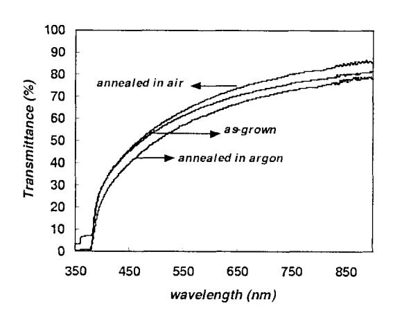
Figure 4 Optical transmittance of doped ZnO thin film
Table 1 Influence of annealing treatment on the band gap and the refractive index of undoped and doped ZnO thin films.
| Sample | Optical Band Gap Eg (eV) | |
|---|---|---|
| Undoped | Doped | |
| as-grown · | 3.19 | 3.17 |
| annealed in argon | 3.19 | 3.17 |
| annealed in air | , 3.11 | 3.15 |
4 Conclusions
- The effect of annealing treatment on the optical and electrical properties of ZnO films was studied based on the discussion on the adsorption and desorption process of oxygen at the grain boundaries of the films.
- The shift of the optical band gap of the film during the annealing treatment in air was related to the change of carrier concentration.
The doped ZnO film showed a more stable optical and electrical properties compared with the undoped film.
5 Acknowledgement
This research was supported by Domestic Collaborative Research Grant (DCRG), which contract number: 015/DCRG/URGE/2000 Directorate General of Higher Education, Ministry of National Education, Indonesia.
6 References
- Yoshikawa, H. & Adachi, S., Jpn. J. Appl. Phys. 36, 1997.
- 2. Dietrich, A. et.al., Thin Solid Film, 122, 1984.
- 3. Baik, Seung Jae, et.al., Appl. Phys. Lett. 70,(26),1997.
- 4. Gupta, Vinay & Mansingh, Abhai, J. Appl. Phys. 80(2), 1996.