

Sari
Epitaksi film GaN dengan MOCVD berbantuan plasma hidrogen
Telah dipelajari efek dari plasma hidrogen pada film GaN, yang ditumbuhkan dengan MOCVD yang dibantu dengan plasma. Film GaN ditumbuhkan di atas safir (0001) tanpa bantuan lapisan penyangga mempunyai struktur polikristalin. Sedangkan film yang ditumbuhkan dengan bantuan lapisan penyangga mempunyai kecenderungan membentuk kristal dengan orientasi tunggal. Telah dicoba untuk menaikkan kecepatan pertumbuhan kristal dengan mengubah-ubah perbandingan TMGa:N. Telah diperoleh kecepatan pertumbuhannya menjadi 450nm/jam bila perbandingan tersebut 1:600, akan tetapi strukturnya memperlihatkan sifat polikristal. Dengan bantuan plasma hidrogen analisis XRD menunjukkan bahwa orientasi film sejajar dengan arah (0002) dan sifat kristalnya dapat diperbaiki.
Kata kuuci: GaN, MOCVD berbantuan plasma, lapisan penyangga, plasma hidrogen, orientasi tunggal.
1 Introduction
GaN and the related material have been particulary attractive for the physical properties and for applications in optoelectronic devices operating from the visible to ultraviolet spectral region1. The nonlinear optical properties of GaN film are also of interest for optoelectronic applications. Several experiment have studied the nonlinear optical properties of GaN films<sup>2-5</sup>, which shows that the GaN crystalline film have large nonlinear optical coefficient. The second-order nonlinear optical coefficient of GaN film grown on sapphire substrate \(d_{33}\) is 33 times the \(d_{11}\) of quartz<sup>5</sup>, and GaN:Mg film has \(d_{33} = -16.5\) pm/V which is 55 times of the \(d_{11}\) of quartz<sup>2</sup>. The large magnitude of the nonlinearities suggested the possibility of new photonics devices based on the III-V nitrides as optical switches. It is known that the nonlinear optical coefficient of a deposited film depend on the film crystalline structure.
In this paper, we report on the studies of the growth method of GaN epitaxial film to achieve better quality.
The GaN epitaxial layer grown by plasma-assisted MOCVD. Plasma-cracked N<sub>2</sub> was used as nitrogen sources to reduce the growth temperature of GaN to 600 - 700°C<sup>6-7</sup>. Moreover we have studied the influence of the buffer layer and hydrogen plasma during the growth. The atomic H irradiation during the growth of GaN by RF-MBE improves the crystal quality of GaN films<sup>8</sup> and also affects the growth mechanism<sup>9</sup>.
2 Experiment
The GaN films studied in this work were grown on (0001) sapphire substrates by plasma-assisted MOCVD system. It consist of a water-cooled stainless-steel vertical reactor equipped with a plasma cracking cell. The reactor was pumped by a combination of a root blower pump and a rotary vacuum pump. The low power downstream plasma cavity (ASTeX) was used to supply reactive-N plasma from \(N_2\) gas and reactive-H plasma from \(H_2\) downward to the substrate. The plasma is generated by 2.45 Ghz microwave of 200 watt and
PROC. ITB, VOL. 33, NO. 1, 2001
uncracked trimethylgallium (TMGa) was used as Ga source. The \(H_2\) carrier gas was purified by passing it throuh a heated palladium cell.
Prior to GaN film growth, the substrate was degreased in organic solvent and was chemically etched in the mixture of \(H_2SO_4\): \(H_3PO_4 = 3\): 1 at 65°C for 10 min and blown with dry nitrogen. The substrate was subjected to thermal cleaning at 600°C for 10 min with hydrogen plasma to remove the contamination and to reduce the surface rougness<sup>10</sup>. The GaN films grown on substrate with and without the buffer layer. After the deposition of a 25 nm thick GaN buffer layer at 450°C, the substrate temperature was raised to the growth temperature of 660°C for the growth of GaN film for 2 hour. The operating pressure was set at 0.5 Torr. In this study, the sample growth conditions are outline in the Table 1.
The structural characterization of the films is carried out by X-ray diffraction using \(CuK\alpha\) radiation. The surface morphology is studied by scanning electron microscopy (SEM). The optical absorption of films were measured at normal incident with UV-vis spectrometer.
Table 1 Detail of the growth conditions
| No. Sample | Flow of TMGa (sccm) | Flow of N2 (sccm) | Buffer layer | Hydrogenation during the growth |
|---|---|---|---|---|
| #(a) | 0.1 | 90 | no | no |
| #(b) | 0.1 | 90 | yes | no |
| #(c) | 0.15 | 90 | yes | no |
| #(d) | 0.15 | 90 | yes | yes, H2 = 10 sccm |
| #(e) | 0.15 | 90 | yes | yes, H2 = 30 sccm |
| #(f) | 0.2 | 50 | yes | yes, H2 = 10 sccm |
3 Result and discussion
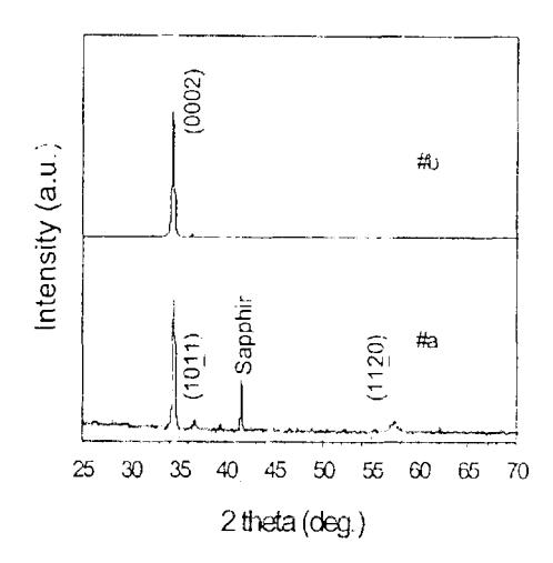
We have studied the effect of the buffer layer on the crystalline structure and the surface morphology of GaN grown on the sapphire substrate without assistance of hydrogen plasma during the growth. The GaN film grown without the buffer layer is composed of mixed crystalline orientation of (0002), (10\(\overline{1}\)1) and (11\(\overline{2}\)0) direction as shown in Fig.1. The GaN grown with the buffer layer have tend to a single crystal orientation of (0002) direction. Fig 2. shows the surface morphology of GaN films grown without and with the buffer layer. The surface morphology of the film grown without the buffer layer is dominated by large hexagonal islands are inhomogenous. Due to the large lattice mismatch and chemical dissimilarity between GaN and sapphire, GaN film growth directly on sapphire results in the nucleation of isolated islands. When the film growth with the buffer layer, the lateral growth is observed. The buffer layer is to promote uniform GaN coverage on sapphire. The full width at half maximum (FWHM) of XRD peak (0002) of sample #a and sample #b are 0.35 deg, and 0.25 deg, respectively. This indicates the crystalline quality of the film growth with buffer layer is better than the film
growth without the buffer layer.
Figure 1 The X-ray diffraction pattern of GaN films grown without and with the buffer layer
Figure 2 Scanning electron microscopy of the surface morphology of GaN films grown without the buffer layer (a) and with the buffer layer (b).
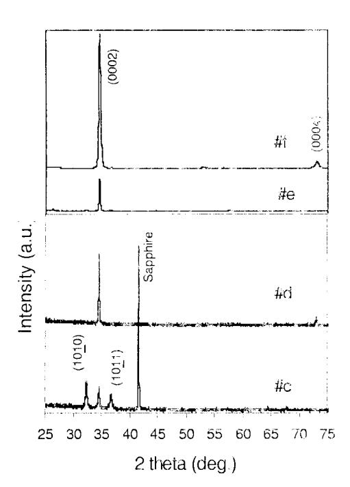
Figure 3 The X-ray diffraction pattern of GaN films grown without (sample #c) and with assistance of hydrogen plasma during the growth (sample #d, #e, #f).
The growth rate of the film with the buffer later (sample #b, III/V ratio = 900) is 0.3 \(\mu\)m/h. We have tried to improve the growth rates of the film by increases the TMGa flow rates of 0.15 secm (III/V ratio = 600). The increasing of TMGa flow rates of 0.15 secm (sample #c) improves the growth rate of 0.45 \(\mu\)m/h, however, the GaN film have a mixture orientation along (10 \(\overline{1}\) 0), (0002) and (10 \(\overline{1}\) i) direction as shown in Fig. 3. We have studied the effect of introducing hydrogen plasma during film deposition to overcome this problem. The film grown with hydrogen plasma during the deposition (sample #d, #e and #f) have the highly oriented (0002) plane parallel with substrate surface. Variation of III/V ratio (sample #f) do not change the XRD pattern as shown in Fig. 3.
The scanning electron microscopy of the morphology of the films is shown in Fig. 4. The surface morphology of the film grown without hydrogen plasma (Fig. 4a) show a random structures, while the films grown with hydrogen plasma have uniform columnar structures (Fig. 4b, c) that are arranged vertically on the substrate (Fig. 4d). Increasing the flow rate of hydrogen plasma from 10 seem to 30 seem increases the diameter of columnar
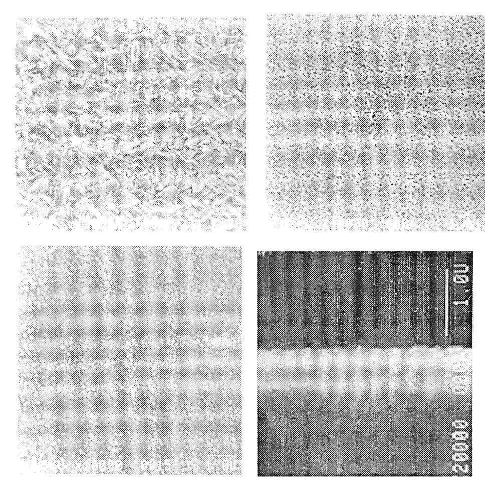
Figure 4 Scanning electron microscopy of the morphology of GaN films grown without (a) and with assistance of hydrogen plasma during the growth of 10 sceni (b) , 30 sceni (c) and the cross section of Fig 4b (d).
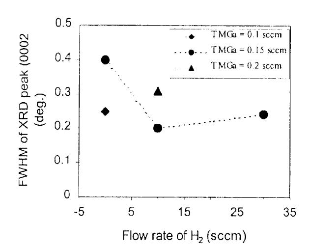
Figure 5 FWHM of XRD peak (0002) of GaN films grown without and with assistance of hydrogen plasma with different parameter deposition.
structure and the surface morphology of the film is homogenous (Fig.4c). The diameter of the columns was about 100 to 200 nm. The FWHM of XRD peak (0002) of sample #c, #d, #e and #f are shown in Fig.5. The best crystalline quality of the sample was the film grown with hydrogen plasma of 10 secm during the growth (sample #d). The difference in surface morphology and crystal structure suggest that hydrogen plasma have a significant effect on the growth kinetic of GaN.
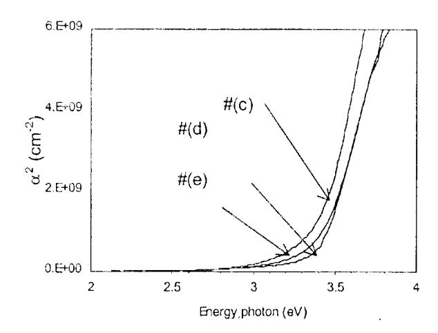
Figure 6 Optical absorption spectra of GaN films grown without and with assistance of hydrogen plasma with different parameter deposition.
Optical absorption measurement were performed at room temperature. Typical result of the optical absorption
spectroscopy measurement of the films which grown with hydrogen plasma during the growth are shown in Fig. 6. The optical bandgap of GaN films grown with hydrogen plasma remain around 3.40 eV, while the sample grown without hydrogen plasma is less then of 3.40 eV. The absorption tail of GaN films grown with hydrogen plasma decrease compared to the GaN film grown without assistance hydrogen plasma. From this result, we believe that assistance of hydrogen plasma during the growth under the optimal conditions is effective to improve the crystal quality.
4 Conclusions
We have studied the effect of hydrogen plasma during the growth GaN film by plasma-assisted MOCVD. GaN film grown without hydrogen plasma at high growth rate shows polycrystalline structure, however those grown with the assistance of hydrogen plasma during the growth the XRD pattern shows a single oriented at (0001)plane. The assistance of hydrogen plasma during the growth is effective to improve the crystal quality.
5 Acknowledgments
This work was supported by The HTTP Program of URGE Project, The Ministry of National Education, The Republic of Indonesia, under contract No: 001/HTTP-IV/URGE/1999 and 019/HTTP-IV/URGE/1999.
6 References
- Strike, S, & Morkoc, H, J. Vac. Sci. Technol. B, 10, 237(1992).
- Zhang, HY, He, XH, & Shih, YH, Appl. Phys. Lett., 69, 2953(1996).
- 3. Schmidt, TJ, & Song, JJ, Appl. Phys. Lett., 72, 1504(1998).
- 4. Haag, H, Gilliot, P, Ohlmann, D, & Levy, R, MRS Internet J. Nitride Semicond. Res., 2, 21(1997).
- 5. Tiginyanu, Kravetsky, IV, MRS Internet J. Nitride Semicond. Res., 5S1, W11.52(2000).
- 6. Sato, M, Jpn.J. Appl. Phys., 34, 1080(1995).
- 7. Sato, M, Appl. Phys. Lett., 68, 935(1996).
- 8. Okamoto, Y, Hashiguchi, S, Okada, Y, & Kawabe, M, Jpn. J. Appl. Phys., 37, L1109(1998).
- Okamoto, Y, Hashiguchi, S, Okada, Y, & Kawabe, M, Jpn. J. Appl. Phys., 38, L230(1999).