

Sari
Penumbuhan GaSb dan AlGaSb dengan MOCVD
GaSb dan AlGaSb adalah semikoduktor paduan yang mempunyai selah energi yang sempit, dewasa ini sangat menarik mengingat penerapannya dalam optoelektronika di daerah inframerah yang dekat dan yang menengah. Perbandingan dari koefisien ionisasi dari lubang dan elektron merupakan faktor yang menentukan dalam APD yang mempunyai respons yang cepat dan derau yang rendah. Dalam tulisan ini penulis melaporkan penumbuhan dari GaSb dan AlGaSb dalam reaktor MOCVD yang vertikal yang telah dibangun sendiri dengan menggunakan trimetilgalium (TMGa), trimetilaluminium (TMAl) dan trisdismetilaminoantimonat sebagai sumbersumber metal-organik. Reaktor tersebut mempergunakan pemandu aliran untuk memperoleh lapisan dengan ketebalan yang uniform. Disini disajikan pengaruh dari temperatur penumbuhan dan perbandingan V/III pada sifat-sifat struktur, morfologi permukaan, sifat-sifat optik dan sifat-sifat listriknya.
Kata kunci: GaSb, AlGaSb, MOCVD.
1 Introduction
Antimonide based compound semiconductors is of current interest due to their potential applications for infra red photodetectors, photonic and high frequency electronic devices and magnetic sensors [1-3]. Ternary and quaternary of GaSb have band gap correspond to wavelengths over a wide spectral range, from 1.24 \(\mu\)m (AlGaAsSb) to 4.3 \(\mu\)m (InGaAsSb), make them suitable material for emitters and detectors in fiber optic communications. On the other hand, the alloy have large ratio of ionization coefficients of hole and electron (\(\beta/\alpha\)) and low excess noise factor. For example by varying the aluminum composition in Al<sub>x</sub>Ga<sub>1-x</sub>Sb from 0.28 to 0.065, the \(\beta/\alpha\) ratio vary between approximately 2 to 20 [4].
High quality of GaSb layers and AlGaSb layers have been grown by Metalorganic Chemical Vapour Deposition (MOCVD) using conventional Ga, Sb and Al precursors, trimethylgallium (TMGa), trimethylantimony (TMSb) and trimethylaluminum (TMAl), respectively [5-6]. However, deposition using TMSb needs relatively high growth temperature due to its high pyrolysis temperature and the films experience carbon contamination, which may be related to the methyl ligands.
Efforts have been made to develop a substitute of Sb precursor that also work at lower growth temperature than that of TMSb. It has been reported that good GaSb layers were grown using tertiarybuthyldimethylantimony (TBDMSb) [7] and triisopropylantimony (TIPSb) at temperature as low as 500°C [8]. However, the growth rate decreases rapidly for growth temperature below 530°C. Recently, a new Sb precursor, tridismethylaminoantimony (TDMASb), has been proposed as an alternative precursor. This precursor has low pyrolysis temperature and is expected to produce low carbon contamination, due to the absence of Sb-C bond and the use of relatively weak bound ligands, even at low growth temperature [9].
Most of MOCVD growths of GaSb and AlGaSb using TDMASb reported to date were carried out at atmospheric pressure. However, there are relatively few reports on the MOCVD growth at low pressure [10]. Growth at low pressure is expected to reduce parasitic gas phase reaction.
In this paper, we report the growth of GaSb, AlGaSb using TDMASb by a homebuilt vertical MOCVD at relatively low pressure (~50 torr) over temperature range of 475 – 580°C. The dependence of the crystallographic orientation, surface morphology, optical and electrical properties on the growth condition to are described.
2 Experiments
A home built MOCVD system with vertical reactor was used for the growth of GaSb and AlGaSb epilayers. The reactor was operated at around 50 torr. A flow guide was used to pre-mix the precursors and to guide the gas flow toward the substrate. The configuration of the flow guide has been optimized to produce uniform layers. The substrate was heated by a resistive type heater which is electronically controlled to provide a stabilized temperature.
The substrate was semi-insulating GaAs (100) and it was prepared using the following procedure. First, the substrate was degrease in boiled trichloroethylene and was cleaned by ultrasonic vibration in acetone and methanol, followed by an etch using (H<sub>2</sub>SO<sub>4</sub>:H<sub>2</sub>O<sub>2</sub>:H<sub>2</sub>O) = 3:1:1 for about 3 minutes. Then, it was rinsed in DI water, dried using nitrogen gas jet and immediately loaded into the reactor. In order to eliminate the residual air in the reactor, the reactor was purged with hydrogen for about 30 minutes.
The TMGa was held at \(-10^{\circ}\text{C}\) and the TDMASb and TMAl were kept in chambers at 29°C in their bubblers. The H<sub>2</sub> carrier gas was purified in a Pd-purifier and introduced into the TMGa bubbler with a flow rate of 8 scem. The H<sub>2</sub> flow rate through the TDMASb and TMAl bubbler were adjusted to explore the optimum growth condition at each growth temperature. The growth temperatures were varied between 475–580°C for GaSb and 540°C–580°C for AlGaSb, while the V/III ratio was adjusted around 1.0.
The crystallographic orientation of the deposited layers were evaluated using X-ray diffraction. The surface morphologies were examined using Scanning Electron Microscopy (SEM) and electrical characterization was performed using Hall-van der Pauw method. The optical transmission spectra was characterized by UV-VIS-NIR Spectrophotometer.
3 Results and discussions
Mirror like GaSb layer were typically 1-3 μm at any V/III ratio and each growth temperature between 510–550°C. The range of V/III ratio which gives good
morphology for III – antimonides was found to be narrow, especially at low growth temperature [11]. However, in this study, that range is even narrower, just around 1.0. We observed Ga- rich phases for lower V/III ratio less than 1.0, which are characterised by the formation of Ga droplets. In other hand, V/III ratio higher than 1.0 produced hillocks shaped, probably due
Figure 1 Typical of SEM micrograph of GaSb layers grown on SI-Gaas at 520°C and various V/III ratio. (a). V/III=0.4, (b). V/III=1.0, (c). V/III=1.2.
Sb-rich phase, similar to that previously reported by other workers [12]. The best surface morphology obtained at V/III ratio of around 1.0 suggested that both Ga and Sb atoms that react to form GaSb on the surface of the substrate are of the same proportion. This proportion was attained probably due to the use of the flow-guide which kept the gas flow inside the flow-guide and directed them to the substrate. Figure 1 show typical surface morphology of GaSb layers grown at 520° at different V/III ratio. At V/III ratio of 0.4, more Ga sources are available than Sb sources produce Ga rich phases deposited in the layer. In contrast, at V/III ratio of 1.2, more Sb sources available than Ga sources, lead to Sb rich layer.
The crystallographic orientation of the GaSb layers were evaluated by X-ray diffraction. For layers grown at temperature between 510–550°C, peaks at \(2\theta = 29.91^{\circ}\)and 61.35° which correspond to (200) and (400) orientation are observed. However, GaSb grown at temperature below 500 °C is amorphous. XRD pattern of GaSb grown at temperature between 510 - 550°C with V/III ratio=1 are shown in figure 2. By increasing temperatures from 510 to 540°C, the intensities of (200) and (400) peaks are increased. The increase of temperature lead to the increase of the activation energy which effectively enhance the formation of GaSb island of similar orientation. This leads to the increase of growth rate, and the intensities of the respective peaks also decrease. It can be seen from figure 2 that GaSb layers grown at 530 and 540°C exhibit high intensity at each peak with narrow Full Width Half Maximum (FWHM) of approximately 0.12°. This indicates that high crystalline phase can be achieved at very narrow growth temperature, between 530 – 540°C.
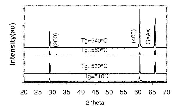
Figure 2 XRD pattern of GaSb thin films grown at different temperature (as indicated) with V/III ratio of 1.0.
Electrical properties of GaSb at room temperature as a function of growth temperature and V/III ratio are shown in figure 3. All layers are p-type, probably caused by either residual impurities in the source or native defects \((Ga_{Sb}, V_{Ga})\) existing in the layer [12]. As shown in figure 3a, the hole concentration slightly increases as growth temperature increases. In contrast, the hole mobility drops significantly as temperature increases. The low
hole concentration and high mobility obtained for the layer grown at temperature between 510–530°C and increases significantly as temperature increases above 540°C. Meanwhile, the hole mobility also slightly increase for layer grown between 510-530°C and drops slightly as the growth temperature is further increased. The low hole concentration and high mobility obtained for the layer grown at temperature around 530°C. Typical of hole concentration and mobility of GaSb grown at temperature are about 10<sup>17</sup> cm<sup>-3</sup> and 600 cm<sup>2</sup>V<sup>-1</sup> s<sup>-1</sup>. These values are comparable to the best values reported by other workers [12].
The typical dependence of hole concentration and mobility on the V/III ratio are shown in figure 3b. Hole concentration slightly increases but mobility decreases as V/III ratio out of 1.0. The high hole concentration of the layer grown with V/III ratio lower or higher than 1.0, probably due to defects formed at Ga or Sb rich conditions as confirmed from the surface morphology examination. Figure 3 suggested that growth conditions which give low hole concentration and high mobility is very narrow, which are at the growth temperature and V/III ratio of around 530°C and 1.0, respectively.
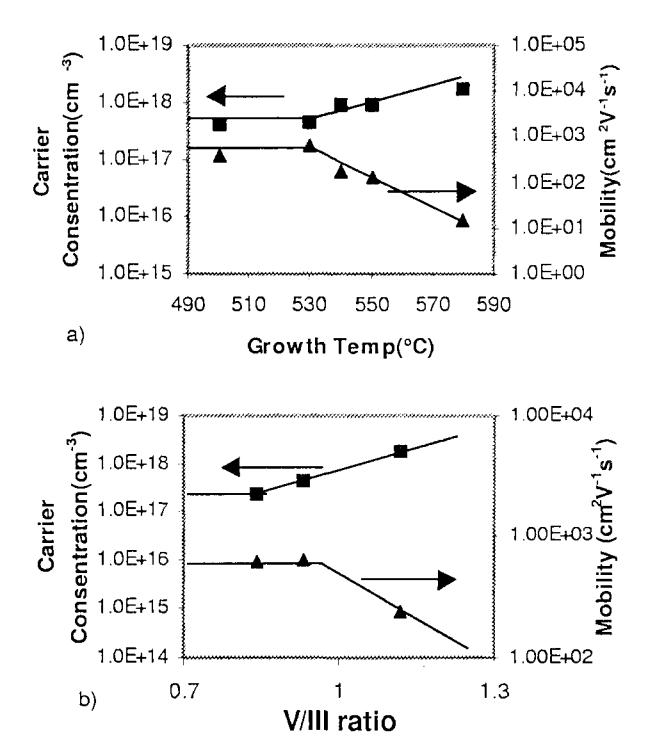
Figure 3 Hole concentration and hole mobility of GaSb layers. (a), grown at different temperature and ratioV/III =1.0. (b) grown at temperature 530° C and different V/III ratio.
The optical transmission spectra of GaSb grown at different growth temperature are shown in figure 4. Transmission spectra of GaSb layer grown at 530°C show sharp transition at around 1700 nm (0.72 eV), which corresponds to the band gap of GaSb, followed by a gradual decrease in transmission until it vanishes at
PROC. ITB, VOL. 33, NO. 1, 2001
around 850 nm. Other samples, grown at 520° and 540°C do not exhibit sharp transition, however, both curves still have the tendency of transition at around 1700 nm, even though the slopes are lower than those of GaSb layer grown at 530°C. The three curves show gradual decrease in intensity for wavelength below 1500 nm which is related to the presence of localized states. The relation between the presence of localized states and growth conditions need to be further investigated. Each transmission spectra do not show interference pattern due
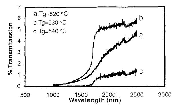
to slightly poor surface morphology.
Figure 4 Room temperature transmission spectra of GaSb thin films grown at various temperature and \(\mbox{ V/III}\) ratio =1.0.
AlGaSb is more difficult to grow than GaSb. The growth started using V/III ratio of around 1.0 and introducing the aluminium flow as low as possible. The growth was carried out between 540-580°C and only AlGaSb grown at 540° C with Al flow rate of 0.2 seem exhibit reasonably good XRD pattern. Others, either exibit amorphous or poor quality of crystallinity. In this study, the effective incorporation of aluminium to form AlGasb alloy still a problem. Figure 5 show the XRD pattern of AlGaSb grown at 540°C with Ga,Sb,Al flow rate of 0.6,0.6 and 0.2 seem, respectively. Two peaks, (200) and (400) are observed, located at \(2\theta = 28.9^{\circ}\) and \(60.6^{\circ}\), respectively. In particular, the (400) peaks is shifted between those of AlSb and GaSb, which are \(60.33^{\circ}\) and
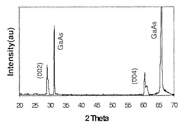
Figure 5 XRD pattern of AlGaSb grown at \(540^{\circ}\)c, flow rate of Ga,Sb and Al are 0.6.0.6 and 0.2 sccm respectively.
61.6°, respectively[13]. This shift is due to the change of lattice constant due to the aluminium content in AlGaSb alloy.
4 Conclusions
GaSb and AlGaSb layers have been grown by vertical MOCVD using TMGa, TDMASb, TMAl as precursors. The optimum growth temperature for GaSb were between 530-540°C and ratio of around 1.0. GaSb layers at optimum growth conditions, have phase dominated by (200) and (400) orientations and good surface morphology. The layer were p-type with the highest mobility of 616 cm²/Vs and hole concentration \(4.4 \times 10^{17}\) cm³ are achieved at growth temperature of 530°C. The growth of AlGaSb mutually depends on growth temperature and flow rate of aluminium. This growth is confirmed by the shift of XRD peak between AlSb and GaSb.
5 Acknowledments
The authors acknowledge the ministry of Research and Technology for research grant under contract no. 008/CG/III/URGE/1997 and RUT no. 40/SP/RUT/1997.
6 References
- Dutta, PS, Bhat, HK, Kumar, V, J. Appl. Phys., 81, (1997) 5821.
- 2. Whitaker, T. Comp. Semicond., 4, (1998) 17.
- 3. Whitaker, T, Comp. Semicond., 4, (1998) 29.
- 4. Juang, Fuh Shyang & Su, Yun Kuin, Prog. Crystal Growth and Charact, 20, (1990)
- Haywood, SK, Henriques, AB, Mason, NJ, Nichols, RJ, & Walker, PJ, Semicond. Sci. Technol., 3, (1988) 315.
- Koljonen, T, Sopanen, M, Lipsanen, H, & Toumi T, J. Electron. Mater., 24, (1995), 1691.
- Chen, CH, Chiu, CT, Su, LC, Huang, KT, Shin, J, & Stringfellow, GB, J. Electron Mater., 22, (1993) 87.
- 8. Chen, CH, Fang, ZM, Stringfellow, GB, & Gedridge, Jr. RW, J. Appl. Phys., 69, (1991) 7605.
- 9. Shin, J, Verma, A, Stringfellow, GB, & Gedridge Jr., RW, J. Crystal Growth, 151, (1995)
- 10. Kuan, Y.K.Su.H & Chang, PH, Solid-State Electronics, 36, 12 (1993).
- 11. Shin, J. Hsu, Y. Hsu, TC, Stringfellow, GB, & Gedridge, RW, J. Electron. Mater., 24, (1995) 1563.
- 12. Wang, CA, Salim, S, Jensen, KF, Jones, AC, J. Crystall Growth, 170, (1995) 55.
- 13. Van der Meulen, YJ, J. Phys. Chem. Solids, 28, (1967) 25.
- 14. XRD log book, Hanawalt