

1 Introduction
Amorphous Silicon (a-Si) material has been widely used in several electronic devices, because this material has several advantages, such as: the energy gap of a-Si can be varied by introducing the carbon ( C ) or nitrogen (N) atom in silicon matrix during the growth process of thin film a-Si (a-Si:H), carrier type (p or n) can be determined by giving impurity to a-Si. Besides, this a-Si material can also be easily grown on a large area at low temperature (200°C). Those advantages make the a-Si material a cheap material to be applied on various semiconductor devices, such as solar cell, thin film light emitting diode (TFLED) and photodiode<sup>1</sup>.
Performance of the various semiconductor devices mentioned above can be enhanced by improving efficiency of light emission and absorption. The usage of double barrier structure constitutes a solution to enhance the efficiency. Previous study have shown that the double barrier structure can increase the injection efficiency of charge carrier (tunneling probability)<sup>2</sup>. Up to now the use of double barrier structure in a-Si device is still very few. Thus the success of this research is expected to contribute to the application of the quantum mechanics based structure in a-Si devices.
2 Result and discussion
The total current density that penetrates a p-i-n a-Si device have been successfully calculated by using a simulation process. The obtained device parameters have been used in fabricating the p-i-n a-Si device with double barrier structure.
2.1 Simulation
When a bias voltage is applied to a p-i-n a-Si device, electron from n-type layer and p-type layer will recombine inside the i-type layer. The electron that enter the double barrier will gain the tunneling probability at resonant state. The tunneling probability (T) of charge carrier was calculated through the Schroedinger equation by using WKB approximation, Green function, and Lorentzian approximation as follow<sup>3-6</sup>.
\[T_{tot} = T_{\text{max}} \frac{\frac{1}{2} \Gamma_{esc} \left[ \Gamma_{is} + \gamma \Gamma_{c} + (1 + \gamma) \Gamma_{esc} \right]}{\gamma (E_z - E_o) + \Gamma^2}\] (1)
In this case, \(T_{max}\) = the maximum tunneling probability without inelastic scattering, \(\Gamma_{esc}\) = contribution of ½ resonant width, \(\Gamma_{is}\) = contribution of inelastic scattering, \(\Gamma_c\) = contribution of scattering due to reflection of hole or electron, \(\Gamma = \Gamma_{is} + \Gamma_{esc}\), \(\gamma\) = damping factor (\(\gamma\) = 1 means elastic scattering, \(\gamma\) = 0 means inelastic scattering), \(E_z\) = energy of incoming electron, and \(E_0\) = resonant energy.
At resonant state, the tunneling probability of charge carrier that pass through the double barrier will eventually approach one. To calculate the resonant energy, the equation proposed by Heading was used as follows<sup>7</sup>.
\[\cos (Kb)\cos(kw)-[(k^2 - K^2)/2kK]\sinh(Kb)\sin(kw) = \cos (n\pi/N)\] (2)
where: \(K = \sqrt{2m(\phi_b - E_o)/\hbar^2}\); \(k = \sqrt{2mE_o/\hbar^2}\); N = number of barrier (in this case N = 2), n = 1, 2, 3, .....etc = energy level in potential well, b = barrier width, \(\phi_b\) = barrier height, and w = width of potential well.
From the equation, the resonant energy appears for a certain variation of b, w, and \(\phi\) only. Figure 1 shows the electron tunneling probability that was varied as a function of bias voltage for several values of b, \(\phi_b\), w, E<sub>0</sub>, with \(\gamma = 0.9\). From the three plot in Fig. 1 it can be seen that maximum value of the tunneling probability is the same. The peak shift occurs for different value of E<sub>0</sub>. The tunneling probability for different value of y is shown in Fig. 2. From the Fig. 2 it can be seen that the tunneling probability reaches the maximum value at energy of the incoming electron is exactly the same as the resonant energy and it can also be seen that the larger y the larger the maximum value of the tunneling probability. This fact tells us that in double barrier structure the elastic scattering is more likely to happen than that of the inelastic scattering.
After obtaining the tunneling probability, the tunneling current density is calculated by using equation proposed by Tsu and Esaki as follows<sup>8</sup>.
\[J_{lun} = \frac{em^{\bullet}}{2\pi^{2}\hbar^{3}} \int_{0}^{E_{F}} dE_{z} T(E_{F} - E_{z})\] for eV \ge EF (3)
\[J_{nun} = \frac{em^*}{2\pi^2\hbar^3} \left\{ V \int_0^{E_F - V} T dE_z + \int_{E_F - V}^{E_F} (E_F - E_z) T dE_z \right\}\] for eV < EF 0.8 0.9 0.9 0.0 0.1 0.2 0.3 0.4 0.5 0.6 Energy of Incoming Electron (eV)
Figure 1 The tunneling probability for b = 1,7 nm, \(\phi_b\) = 0,3 eV, w = 6,5 nm and E\(_0\) = 0,28 eV.
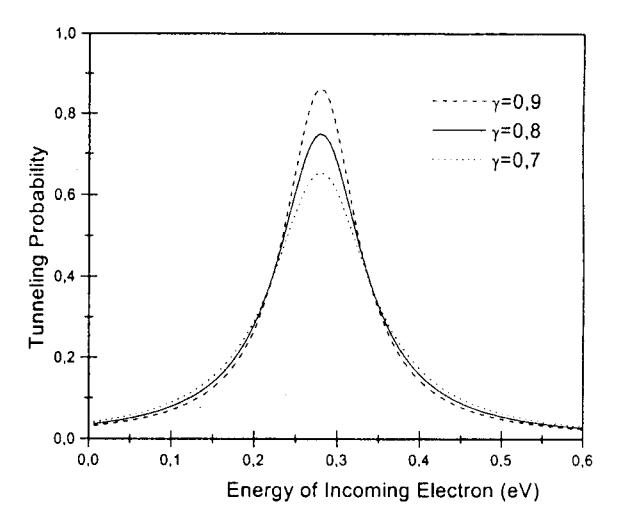
Figure 2 The tunneling probability for b = 1.7 nm, \(\phi_b = 0.3\) eV, w = 6.5 nm and \(E_0 = 0.22\) eV.
where \(E_F\) = the Fermi energy, V bias voltage. The result of the calculation of the tunneling current density is presented in Fig. 3. Figure 3 shows that pattern of the tunneling current density follows the pattern of the tunneling probability.
Total current density that penetrates the device is a sum of the tunneling current density and diffusion current density. The diffusion current density is due to the difference of charge carrier concentration between p-i layer and n-i layer. The diffusion current density comes from recombination of hole from n-type layer and electron from p-type layer. By applying bias voltage to the device, holes and electrons will be injected into the i-type layer and recombine in the i-type layer.
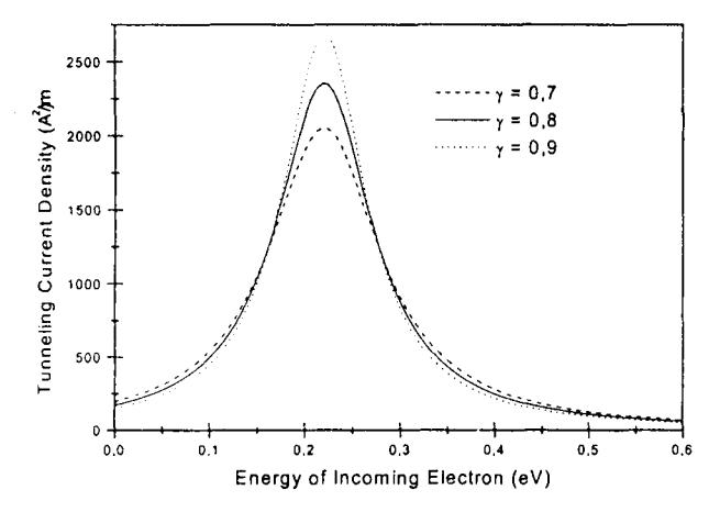
Figure 3 The tunneling current density for b = 1,7 nm, \(\phi_b\) = 0,3 eV, w = 6,5 nm and E<sub>0</sub> = 0,28 eV.
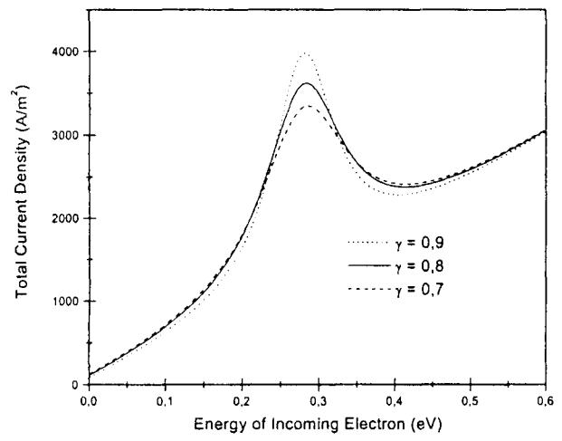
Figure 4 The total current density for b = 1,7 nm, \(\phi_b\) = 0,3 eV, w = 6,5 nm and E\(_0\) = 0,28 eV.
The calculation of the diffusion current density was started from equation for built-in potential \((V_{bi})\) that was obtained from equation for drift current, and then the density of minority charge carrier was calculated at each layer. Afterward, the diffusion current density was finalized by using basic equation of continuity for electron and hole, basic equation for electron density and hole density, and equation of recombination rate, so that we got equation for diffusion current density, as follows.
\[J_{dif} = \left(\frac{qD_p p_{no}}{L_p} + \frac{qD_n n_{po}}{L_n}\right) \left(e^{qV/kT} - 1\right)\] (5)
where \(D_p\), \(D_n\) = coefficient of diffusion for hole and electron respectively; \(L_p\), \(L_n\) = diffusion length for hole and electron; \(n_{po}\) = the thermal equilibrium of electron concentration in the p-type layer; \(p_{no}\) = the thermal equilibrium of hole concentration in n-type layer. Finally the total current density that passes through the device is a sum of the total tunneling current density and the diffusion current density, and it can be expressed as follows.
\[J = J_{\text{tun}} + J_{\text{dif}}\] and plot of the total current density is depicted in Fig. 4.
From Figs.3 and 4 it can be seen that peak of the total current density gain 1.5 as high as peak of the tunneling current density. The total current density will increase after decreasing at energy of incoming electron of 0.40 eV so that the peak to valley current ratio (PVCR) reaches 1.875. From Fig. 4 it can also be seen that the total current density reaches the maximum value 3950 A/m<sup>2</sup> at energy of incoming electron of 0.28 eV or 0.56 volt of bias voltage.
2.2 Experiment
2.2.1 Optimization of energy gap (E<sub>g</sub>) of the barrier
The barrier height in the p--n a-Si device is equal to \(\frac{1}{2}\) (Eg barrier – Eg layer-layer). The barrier energy gap can be varied from 1,8 eV up to 2,36 eV by adjusting ratio of CH<sub>4</sub> to CH<sub>4</sub> + SiH<sub>4</sub> as shown in Fig. 5. From Fig. 5 it can be seen that the barrier energy gap will increase as the ratio increases. In other word, the barrier energy gap increases as the content of C and Si is increased. This fact is due to the binding energy of the Si-C is higher than that of Si-H.
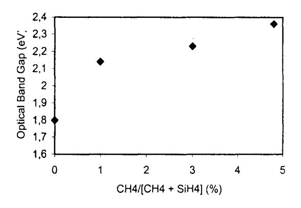
Figure 5 Variation of the barrier energy gap (a-SiC:H).
2.2.2 Current density of the p-i-n a-Si device
The fabricated double barrier structure of p-i-n a-Si consists of several layer. There are glass substrate/p-a-Si:H (140 Å;2.15 eV)/i-a-Si:H (1800 Å; 1.81 eV)/barrier a-SiC:H (45 Å; 2.36 eV)/i-a-Si:H (potential well, 1800 Å; 1.81 eV)/ barrier a-SiC:H (45 Å; 2.36 eV)/i-a-Si:H (1800 Å; 1.81 eV)/ )/n-a-Si:H (300 Å; 1.81 eV)/Al. As a comparison we also fabricated p-i-n a-Si device without double barrier with i-type layer width is a sum of barrier width and i-type width inside double barrier structure of p-i-n a-Si. From our measurement of I-V characteristic, it can be seen from Fig. 6, that p-i-n a-Si device with double barrier show a peak current at 0.55 volt of bias voltage is equivalent to twice as high as resonant energy, while p-i-n a-Si without double barrier does not have any peak.
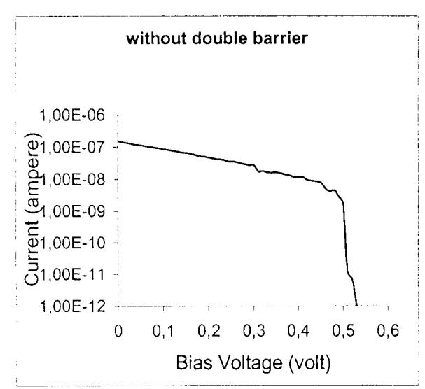
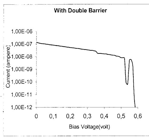
Figure 6 l-V caharacteristic of p-i-n a-Si device.
3 Conclusion
We can conclude our result as follows:
l. The study of simulation and fabrication of p-i-n a-Si device with double banier structure has been successfully canied out.
- The resonant energy of the double barrier structure only appeared for a certain value of barrier width, barrier height and potential well width. z.
- 3 . Maximum value of current density lrom simuiatron appeared at 0.28 eV or equal to 0.56 volt.
- The current peak obtained fiom measurement of I-V characteristic was in a good agreement with simulation result. 4.
Acknoledgement
This research was supported in part by Domestic Collaborative Research Grant (DCRG), which contract number 014/DCRGruRGE/2000, Directorate General of Higher Education, Ministry of National Educatrcirr, Indonesia.
References 5
- Wenas, Wilson W., The 3'd Lltorkhop on Electro-Contnrunication and Inforntation (WECI-lll.), Bandung, (1999). l .
- 2. Hamidah, Ida, The 3'd lltorkshop on Electro-Communication and Infornnlion (WECI-lll), Bandung, (1999).
- Takahashi, K, dan Konagai, M, Amorphous Si/icon Solar Cells, North Oxford, Great Britain, pp. 97 r63, (1e86).
- Garcia Calderon, The Physics of Low Dimensional Semiconductor Structure, Plenum Press, New York. pp. 107 - 1 16, (1991). 3 .
- Ricco, B, & Azbel, M.Ya, Physicul Review B. 29, pp. 1970-1981, (1984). A
- Sze, SM, Senrlconductor Det,ices: Plrysics antl Technologt. John Wiley & Sons, Singapore, pp. 30- 97, (r985).
- 6. Booker, SM, et. al. Semicond. Sci. Technol.,7, pp. 8439-844 r , (t992),
- 1. Collins, S, ct. al., J. Appl. Phys., 63, (1), pp. la2 r4e, (1e88).
- 8. Tsu, R, & Esaki, L, Appl. Ph.ys. Letter,22, 191J, 562.