
1 Introduction
Metal-oxide semiconductors, e.g. Zn–O, In–Zn–O and Ga–In–Zn–O (abreviated as GIZO) thin films, have been extensively investigated for optoelectronic applications such as flat panel displays, transparent electrodes in solar cells, and transparent thin film transistors [1]. Transparent oxide-based transistors for display using GIZO as channel materials show high mobility over amorphous silicon thin film transistors (TFTs). High-performance GIZO TFTs, fabricated on plastic, cellulose paper, and flexible substrates, provide high field-effect mobility (>10 cm2/V s), low processing temperature (<250°C), great potential for low-cost and large-area deposition [2,3].
Recently, it has been reported that high-performance TFTs were made with amorphous gallium indium zinc oxide a-GIZO channel layers treated by argon, oxygen, and N<sub>2</sub>O plasma in order to improve the contact resistance and instability under light illumination [4,5]. The surface states under different ambient gasses and degradation behavior under hot carrier stress for InGaZnO TFTs have also been investigated [6,7]. In addition, hydrocarbon impurities in GIZO, inevitably incorporated during deposition, have a negative effect on device performance. One way to reduce the residual hydrocarbon from the GIZO is to adopt the chlorine plasma treatment because chlorine can easily react with carbon and hydrogen to form CCl4and HCl, respectively [8,9]. Chlorine can also substitute oxygen on the surface of ZnO thin films in order to increase band gap and electrical properties [10]. The control of oxygen deficiency by adjusting the oxygen supply during deposition is crucial to achieve the optimum properties for use as the channel material in TFTs. The influence of oxygen deficiency on the electronic structure of an a-GIZO using rf-Magnetron sputtered GIZO TFTs has been reported [11,12].
The electronic properties of GIZO thin films are essential for understanding the transport properties of TFT devices based on GIZO. So far, the effect of chlorine plasma treatment on the electronic properties of GIZO has not been experimentally investigated. Therefore, in this work we have studied the effect of chlorine plasma treatment on the electronic properties of as-grown and treated GIZO films as a key to electrical properties using secondary ion mass spectroscopy (SIMS), reflection electron energy loss spectroscopy (REELS), and X-ray photoelectron spectroscopy (XPS) measurements. The atomic concentration ratio Ga:In:Zn~2:2:1 with variations in O2/(O2+Ar) concentration are 0, 2, and 8%, respectively.
2 Experiment
GIZO thin films were deposited by rf magnetron sputtering on SiO2/Si substrates with an rf power of 200 W at room temperature in an argon gas ambience containing 0%, 2%, and 8% of oxygen. The XPS and REELS spectra were obtained using a VG ESCALAB 210. They were measured using an Al source with a pass energy of 20 eV. The incident and takeoff angles of electrons were 55° and 0° from the surface normal, respectively. The XPS binding energies were referenced to C 1s peak of carbon contamination at 284.5eV. The REELS were measured with a primary electron energy of 1.5 keV for excitation and with a constant analyzer pass energy of 20 eV. The full width at half maximum (FWHM) of the elastic peak was 0.8 eV. The depth profiles of GIZO were measured using SIMS.
3 Results and Discussion
We made use of the REELS measurement to find the band gap. Figure 1 shows the REELS spectra for GIZO thin films. The band gap values were determined from the energy loss spectrum; this method is described in Ref. [13-17]. It is noted that the bandgap of the Cl2 plasma treated GIZO films increased 0.3 eV. We attribute this phenomenon to the band gap of the binary endpoint of GIZO owing to an In2O3 decrease in GIZO thin films. It is known that crystalline ZnO has a band gap of about 3.37 eV [18], crystalline In2O3 has a direct band gap of around 3.6 eV, and an indirect bandgap of 3.1-3.3 eV [19], and crystalline Ga2O3 has a band gap of about 5 eV [20]. For GIZO, plasma peaks appear at 11, 19.8, 26, and 55 eV. A strong plasmon peak appears at 19.8 eV. Another broad plasmon peak appears around 55 eV away from the elastic peak center.
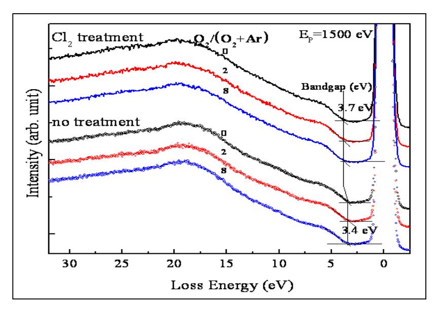
Figure 1 Reflection electron energy loss spectra of GIZO thin films for the primary energies of 1500 eVb.
Figure 2(a) shows narrow scans of the In 3d5/2 peaks. The chemical states of In2O3 and In(OH)3 were detected on the surface of the untreated specimen, which corresponded to binding energies of 444.6 and 444.8 eV, respectively. For the Cl2treated GIZO specimens, the main peaks were shifted to a higher binding energy of approximately 445.1 eV. According to the data reported in the literature, the binding energy of In2O3 is in a range of 444.3–444.9 eV and that of InCl3 in a range of 444.6–445.3 eV [21]. Therefore, it is reasonable to conclude that Cl radicals replace O atoms forming InCl3 compound that exists on the surface of the chlorine plasma treated GIZO thin film. The parameters deduced from Figure 2 are summarized in Table 1 for clarity.
Table 1 XPS binding energy states of \(In_{5/2}\), \(Ga_{3/2}\), and \(Zn_{3/2}\) core level.
| O2/(Ar+O2) (%) | Binding Energy States (eV) | |||||
|---|---|---|---|---|---|---|
| In 3d5/2 | Ga 2p3/2 | Zn 2p3/2 | ||||
| No Treatment | Cl2 Treatment | No Treatment | Cl2 Treatment | No Treatment | Cl2 Treatment | |
| 0 | 444.6 | 445.1 | 1117.5 | 1117.8 | 1021.6 | 1022 |
| 2 | 444.8 | 445.1 | 1117.7 | 1117.8 | 1021.7 | 1022 |
| 8 | 444.6 | 445.1 | 1117.4 | 1117.8 | 1021.6 | 1022 |
| In2O3 and In(OH)3 | \(InCl_3\) | \(Ga_2O_3\) | \(Ga_2O_3\) | ZnO | \(ZnO_xCl_y \ ZnCl_2\) | |
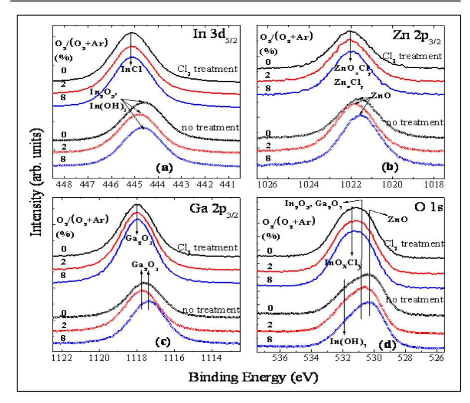
Figure 2 In \(3d_{5/2}\), Ga \(2p_{3/2}\), Zn \(2p_{3/2}\), and O 1s core level photoelectron spectra for GIZO thin films.
Figure 2(b) shows the narrow scans of the Zn 2p3/2 peaks. The peak positions of the Zn 2p3/2 (1021.6-1021.7 eV) of the untreated GIZO surface were shifted toward a higher binding energy by ∼0.4 eV compared with those of the untreated GIZO, as shown in Figure 2(b). This indicates that a chemical reaction occurred between Zn and Cl on the surface. During the plasma treatment, Cl radicals reacted preferentially with the Zn atoms in the GIZO layer leading to the formation of zinc oxychloride (ZnOxCly), or Cl radicals replaced O atoms, forming zinc dichloride (ZnCl2) bonds as a result [22,23].
Figure 2(c) shows the narrow scans of the Ga 2p3/2 peaks. The as-deposited thin films show chemical states of Ga2O3 at binding energies of 1117.4 - 1117.7 eV, and, after treatment with Cl2, the binding energy was shifted to 1117.8 eV. The binding energy of Ga2O3is in a range 1116.9 – 1117.8 eV [24], indicating that Cl radicals during plasma treatment were not bonding with Ga cations on the surface of the GIZO thin films.
The O 1s spectra in Figure 2(d) show that there is a peak in the range of 530.3- 530.8 eV. These are binding energy ranges for O bonding with In, Ga, or Zn cations. For the untreated sample, a peak appears at a binding energy of around 531.8 eV indicating the bonding of O with H. Here, the bonding between O and H is related to the formation of In(OH)3 bonds caused by surface contamination of the GIZO thin films by the hydroxyl groups due to air exposure. The chlorine plasma treatment samples show that the In–O and Zn–O bonding becomes negligible, which demonstrates the formation of In–Cl and Zn–Cl bonding on the surface as a result.
The secondary ion mass spectroscopy (SIMS) depth profiles of GIZO for different ratios of O2/(O2+Ar) are shown in Figure 3(a) and 3(b) to be 2% and 8% respectively. It can be observed that the change in the surface concentrations of InO and ZnO occurs for the samples that had plasma treatment. Meanwhile, in the case of GaO, the surface atomic compositions are nearly constant unlike the untreated samples. These results show that the Cl radicals did not react with the Ga atoms on the surface of the GIZO thin films. This is consistent with the XPS data, as shown in Figure 2(c). On the other hand, the decreased InO, ZnO, OH and O2 on the surface of GIZO are due to the oxygen deficiency on the surface. Additionally, the drastic decrease of InO and OH can be understood in terms of the formation of InClx and volatile HCl as a reaction by-product after Cl2 plasma treatment. Chlorine can also easily react with carbon to form CCl4. With chlorine plasma treatments, therefore, it is expected that the carbons and hydrogen incorporated in GIZO diffuse out of the transparent thin films.
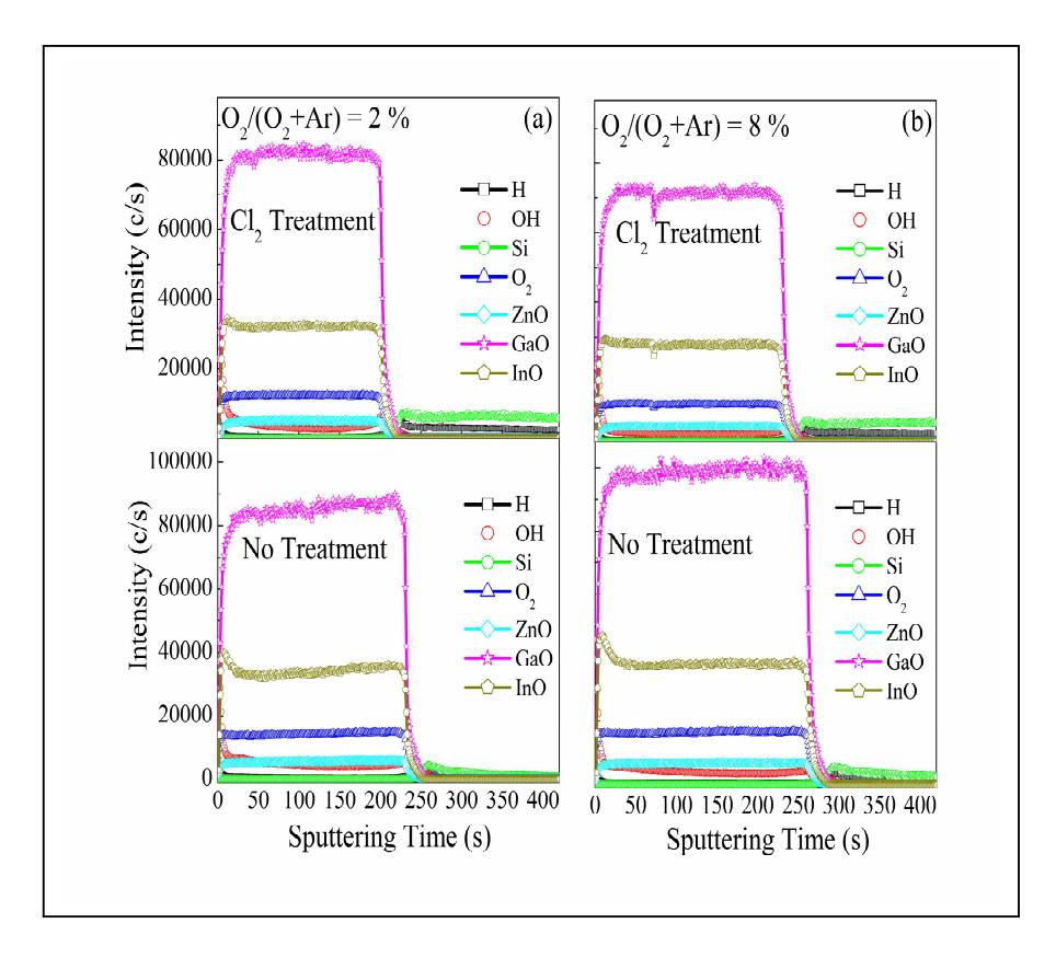
Figure 3 Secondary ion mass spectroscopy of GIZO thin films for 2% and 8% of O2 /(O2+Ar).
The InO concentration in the Cl2 plasma treated surface decreased drastically. GaO was relatively stable but O2 and ZnO were relatively low compared with untreated samples. Therefore, the change of the bandgap (REELS spectra) and chemical shift (XPS spectra) with Cl2 plasma treatment comes from the oxygen deficiency and the hydrocarbon impurities were reduced on the GIZO film surface. Energetic Cl ions during plasma treatment are known to induce the relatively light atoms from the surface as a result of the physical momentum transfer between the ions in the plasma and the atoms on the surface [25]. Therefore it is quite reasonable to assume that the hydrocarbon impurity on the GIZO film surface is preferentially dissociated by the Cl ion forming bonds with In and Zn cations.
4 Conclusions
We have investigated the electronic structures and chemical states for GIZO thin films with Cl2 plasma treatment and compared as-deposited GIZO thin films via REELS and XPS analysis. The depth profiles measured using SIMS indicated a decrease of the concentration of InO and ZnO, and GaO was relatively stable after chlorine plasma treatment. Chlorine radicals were formed on the surface of the GIZO, and they formed bonds with In and Zn cations. The band gap increased 0.3 eV after Cl plasma treatment, indicating hydrocarbon contamination decrease and oxygen deficiency on the surface of the GIZO thin films.
Acknowledgements
This research was supported by Basic Science Research Program through the National Research Foundation of Korea (NRF) funded by the Ministry of Education, Science and Technology (2012R1A1A2009590).